
Spatial light modulator features
a spatial light modulator and features technology, applied in the field of heat-minimizing spatial light modulators, can solve the problems of extremely long development time for prototyping any kind of electronic circuit, increased mask cost for integrated circuit fabrication, and inability to meet the needs of the user, so as to achieve the effect of eliminating the source and higher resolution
Patent Information
- Authority / Receiving Office
- US · United States
- Patent Type
- Applications(United States)
- Current Assignee / Owner
- Publication Date
- 2008-01-24
Smart Images
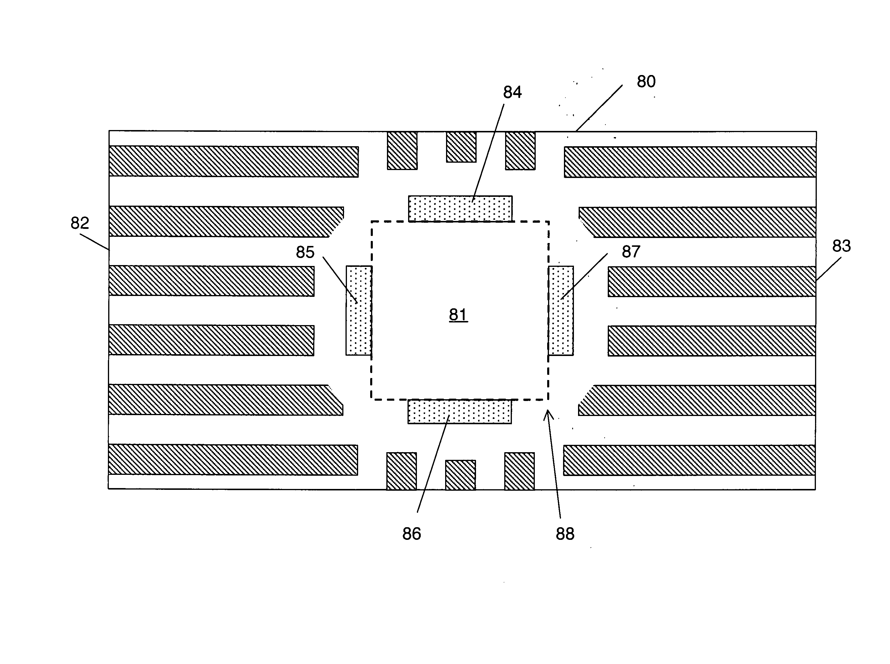
Figure 1 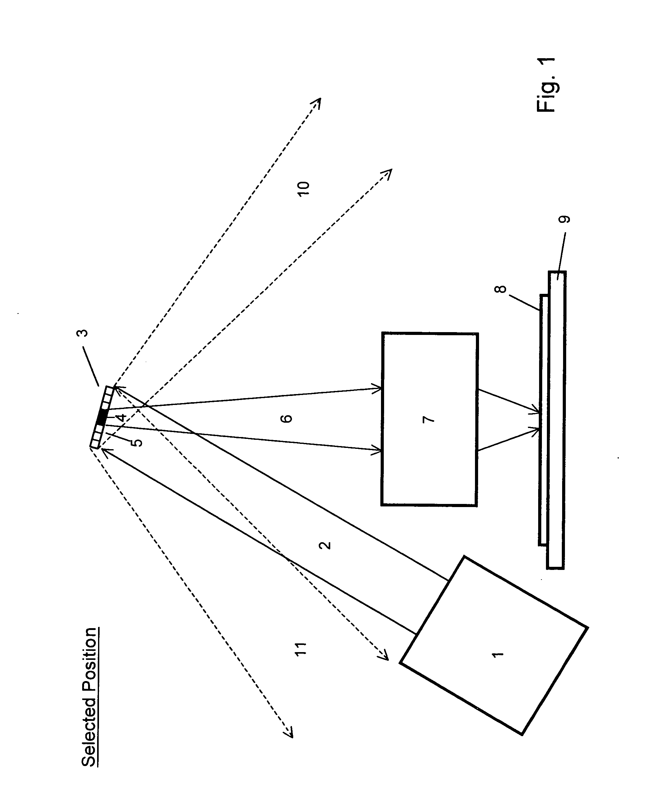
Figure 2 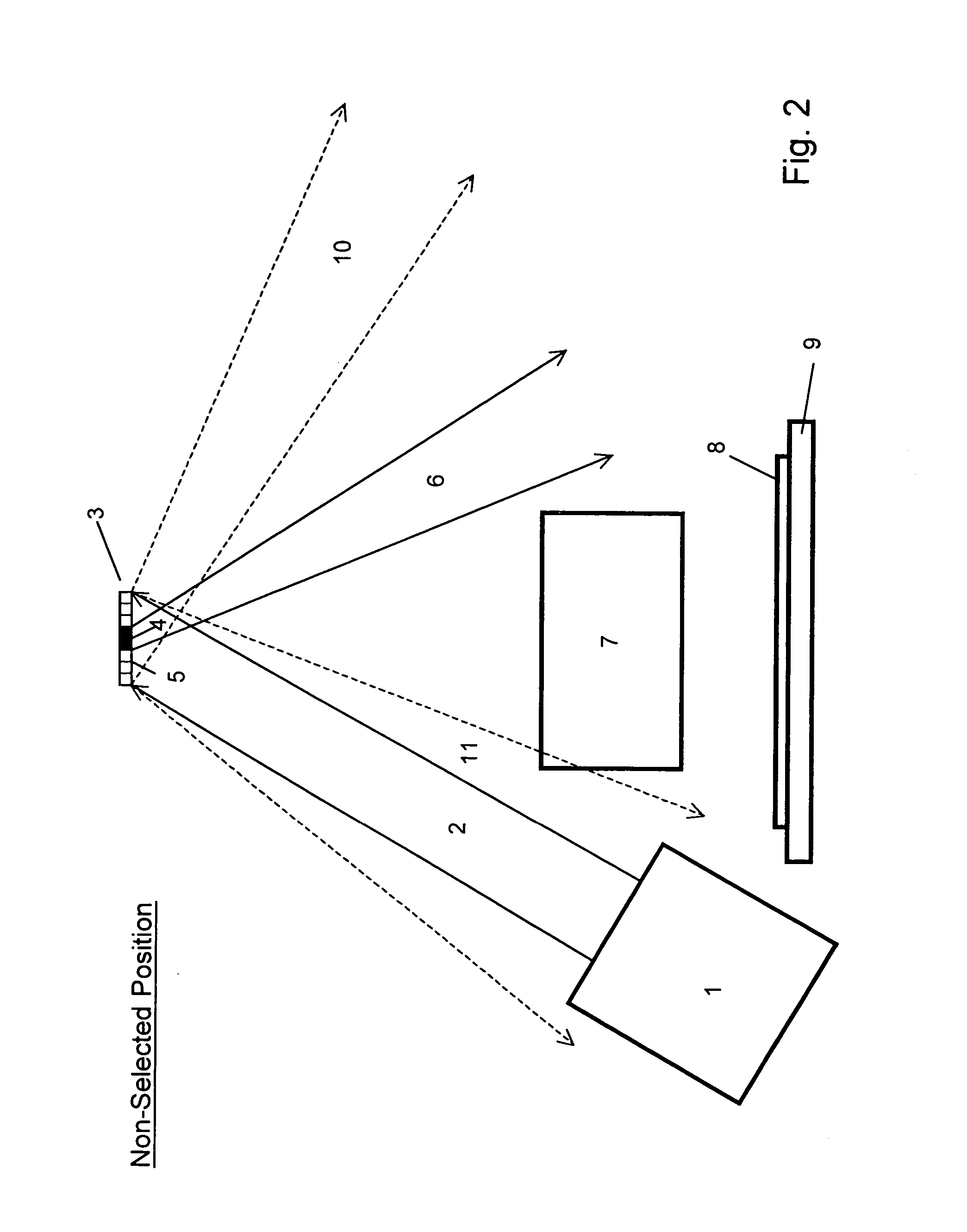
Figure 3
Abstract
Description
CROSS-REFERENCE TO RELATED APPLICATIONS
[0001] This is a divisional application of U.S. patent application Ser. No. 11 / 237,382, filed Sep. 28, 2005, now U.S. Pat. No. ______, Issue date ______, Jain et al., SPATIAL LIGHT MODIULATOR ARRAY WITH HEAT MINIMIZATION AND IMAGE ENHANCEMENT FEATURES.BACKGROUND OF THE INVENTION
[0002] (1) Field of the Invention
[0003] This invention relates to a heat-minimizing spatial light modulator with image enhancement features based on diffracting digital micromirror devices (DDMDs) and to techniques for fabricating and incorporating DDMDs in projection optical imaging and patterning systems.
[0004] (2) Description of the Related Art
[0005] A maskless lithography technology that is capable of high-resolution patterning is essential for manufacturing of many microelectronic and bio-molecular devices. Lithographic techniques using conventional masks involve a multi-step process which includes defining the desired features on the mask which is then used to...
Examples
Embodiment Construction
[0029] General Considerations
[0030] Spatial light modulator (SLM) arrays are used in maskless lithography and other applications. A variety of SLMs have been employed for use with different wavelengths. The most widely investigated type of SLM comprises a 2-D array of micromirrors fabricated in Si wafers with process technologies similar to those used in IC production. In these SLMs, typically the size of an individual micromirror element (pixel) is approximately 15×15 μm. When used in lithography, the achievable system resolution and throughput depend on the pixel size and number of pixels. It is highly desirable to make the size of each pixel as small as possible and the number of pixels in an SLM array as large as possible. For example, with advanced microelectromechanical systems (MEMS) technologies, it is possible to make an SLM array with a grid size of 4×8 μm, with a total number of micromirrors as large as 108-109.
[0031] By minimizing the size of the pixels, it is possible...