
Photovoltaic module-mounted ac inverter
a photovoltaic module and inverter technology, applied in the direction of electric variable regulation, process and machine control, instruments, etc., can solve the problems of unsatisfactory reactive power, no power is efficiently transferred from the inverter into, and minimal impact on the total power produced by the pv system, so as to reduce the current requirements of the inductors, increase ripple frequency, and reduce the effect of current requirements
Patent Information
- Authority / Receiving Office
- US · United States
- Current Assignee / Owner
- Publication Date
- 2008-11-20
Smart Images
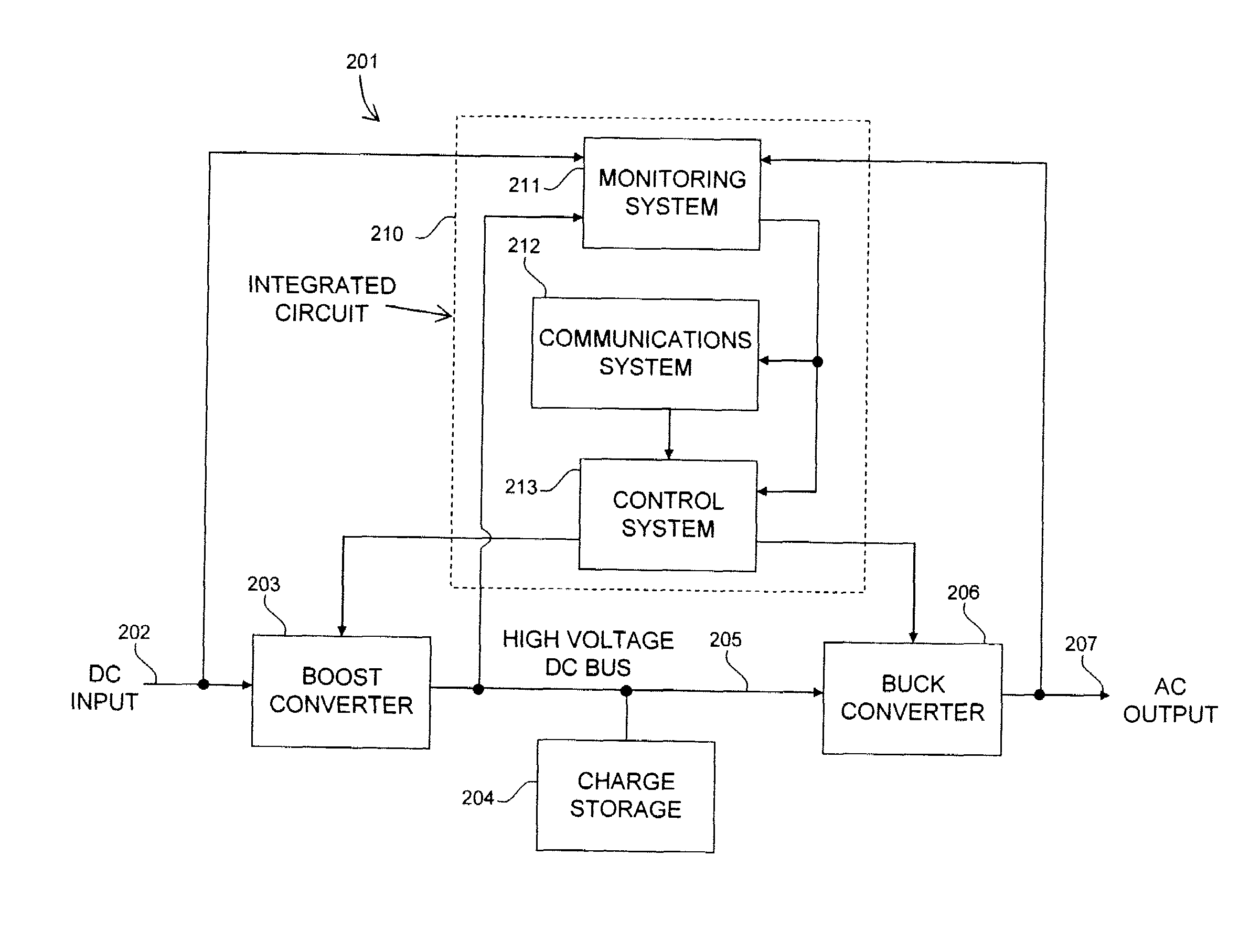
Figure 1 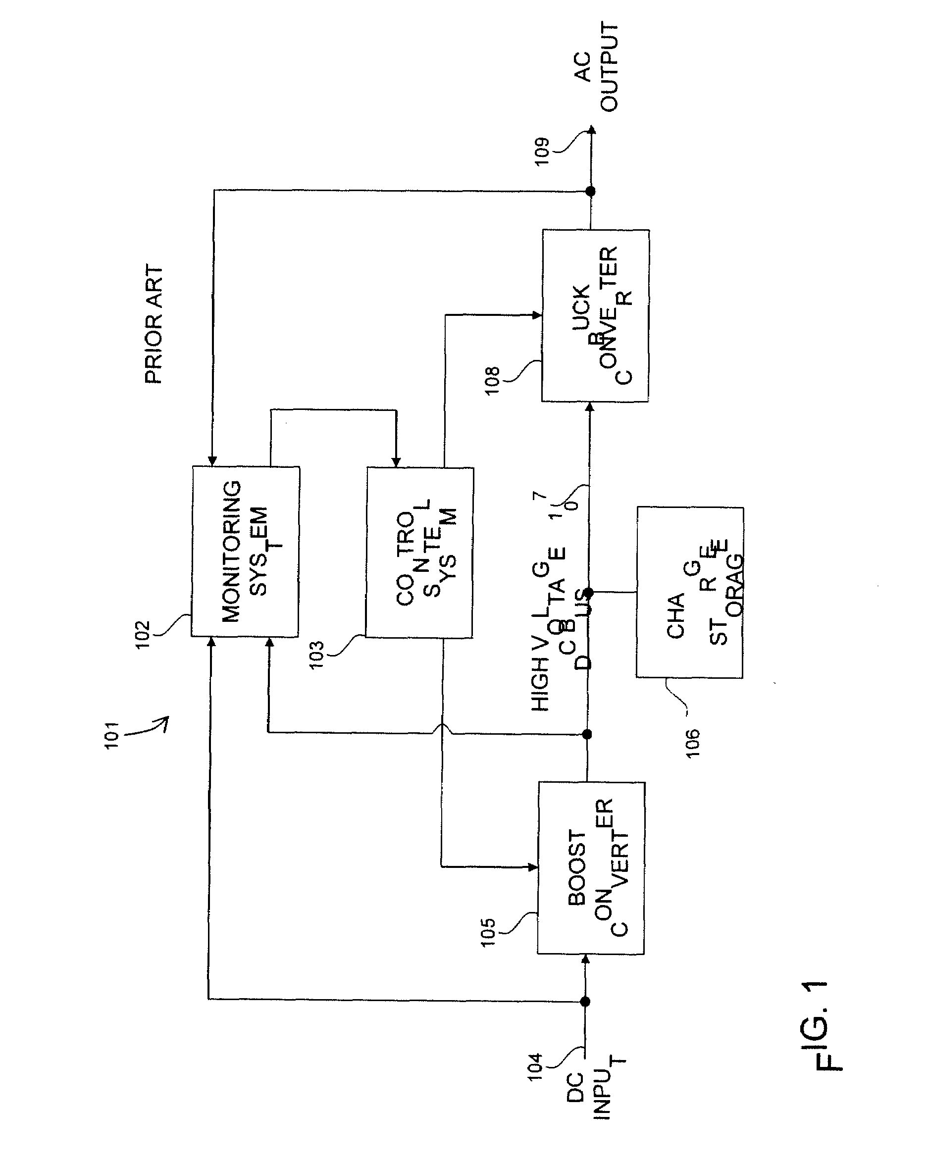
Figure 2 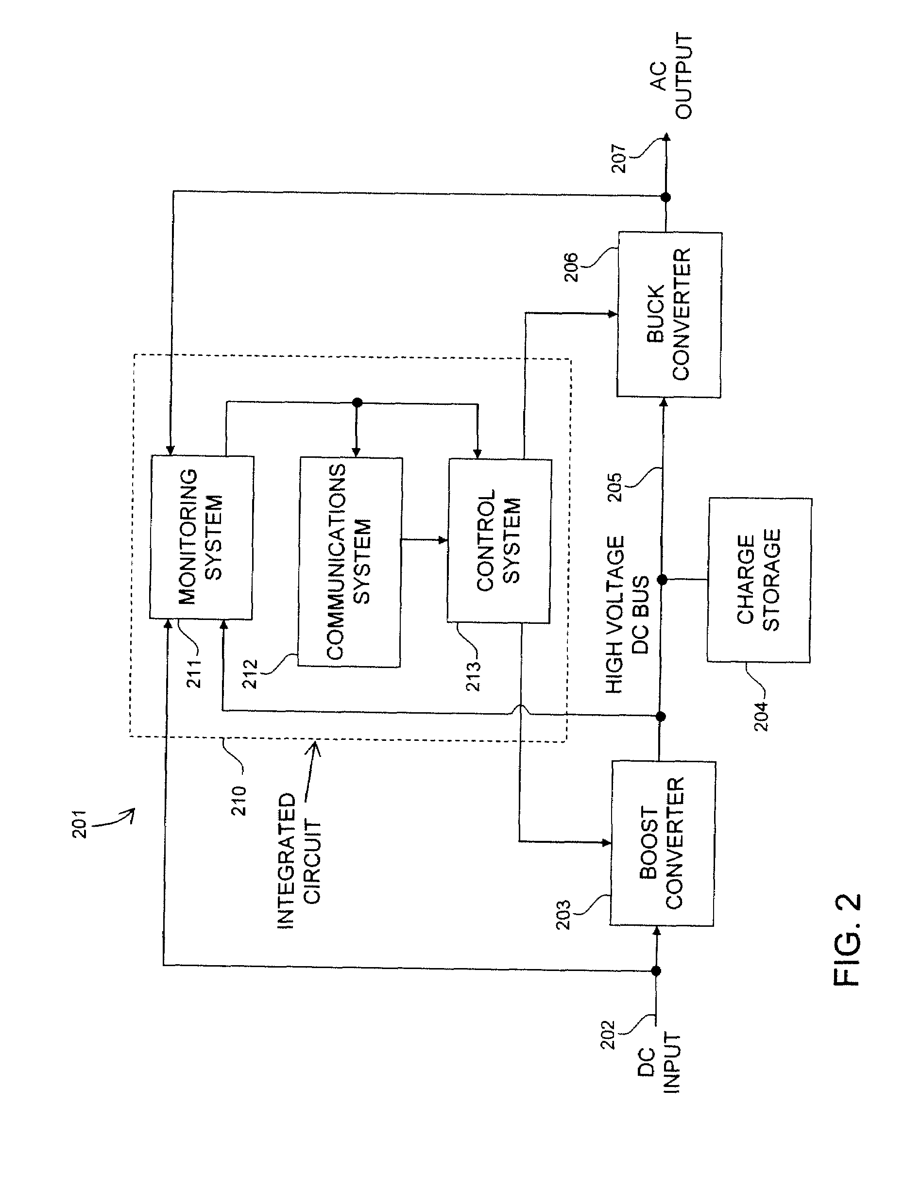
Figure 3
Abstract
Description
RELATED APPLICATION
[0001] The present application relates to and claims the benefit of priority to U.S. Provisional Patent Application No. 60 / 938,663 filed May 17, 2007, which is hereby incorporated by reference in its entirety for all purposes as if fully set forth herein. The present application is further related to co-pending U.S. Patent Application Ser. No. LAR004 entitled, “Photovoltaic AC Inverter Mount and Interconnect” and U.S. Patent Application Ser. No. LAR002 entitled “Distributed Inverter and Intelligent Gateway”, both of which are hereby incorporated by this reference in their entirety.BACKGROUND OF THE INVENTION
[0002] 1. Field of the Invention
[0003] The invention relates to direct current to alternating current power conversion and, more particularly, to photovoltaic module output power conversion to alternating current.
[0004] 2. Description of the Related Art
[0005] An inverter is a device that performs direct current (DC) to alternating current (AC) power conversion. FIG....
Examples
second embodiment
[0039]Referring now to FIG. 7, a tandem single-inductor, bipolar-output boost converter 701 according to the present invention includes a DC input 702, a first input switch PWMI1703, a first input switch current ISW1730, a first ground switch PWMG1708, a first negative output diode 704, a first negative output diode current IDN1731, a negative output DC voltage 705, a negative output capacitor 707, an inductor 706, a first positive output diode 709, a first positive output diode current 732, a positive output DC voltage 710, a positive output capacitor 711, a second input switch PWMI2723, a second input switch current ISW2733, a second ground switch PWMG2728, a second negative output diode 724, a second negative output diode current IDN2734, a second positive output diode 729, a second positive output diode current 735 and a ground terminal 713. Components 702, 703, 704, 705, 706, 707, 708, 709, 710 and 711 comprise a first single-inductor, bipolar-output boost converter. Components...
first embodiment
[0040]Referring now to FIG. 8, a timing diagram of a single-inductor, bipolar-output boost converter operating in two-cycle mode 501 according to the present invention includes waveforms for signals PWMI1802, PWMG1803, first switch current ISW1804, first inductor current IL1805, first positive output diode current IDP1806, first negative output diode current IDN1807, signals PWMI1808, PWMG1809, second switch current ISW1810, second inductor current IL1811, second positive output diode current IDP1812, second negative output diode current IDN1813, positive DC output voltage +VDC 814 and negative DC output voltage −VDC 815. The description of the signals and their relationships is given in the description for FIG. 7. The timing diagram 801 shows one possible result and a person skilled in the art will recognize that the relative timing and signal level scales can be adjusted over a large range with no change in fundamental circuit behavior. The first inductor 706 and the second induct...