
Inspection method for semiconductor wafer for reviewing defects
a technology of semiconductor wafers and defects, applied in the direction of material analysis, instruments, and wave/particle radiation, can solve the problems of poor adhesive electrical defects in some cases, and film easy to be easily peeled off, so as to effectively observe the edge of the wafer
Patent Information
- Authority / Receiving Office
- US · United States
- Patent Type
- Applications(United States)
- Current Assignee / Owner
- Publication Date
- 2009-02-19
- Estimated Expiration
- Not applicable · inactive patent
Smart Images
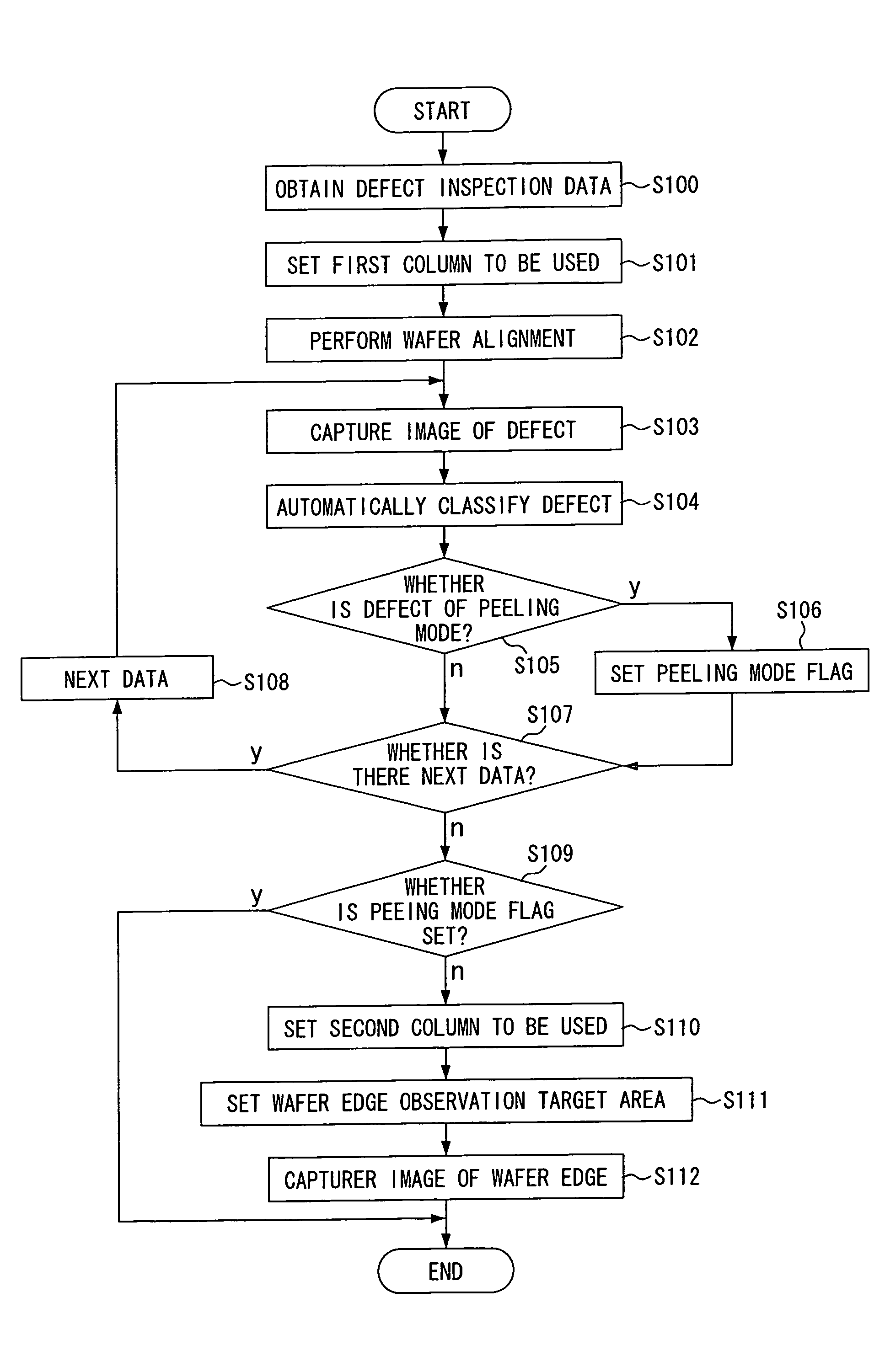
Figure 1 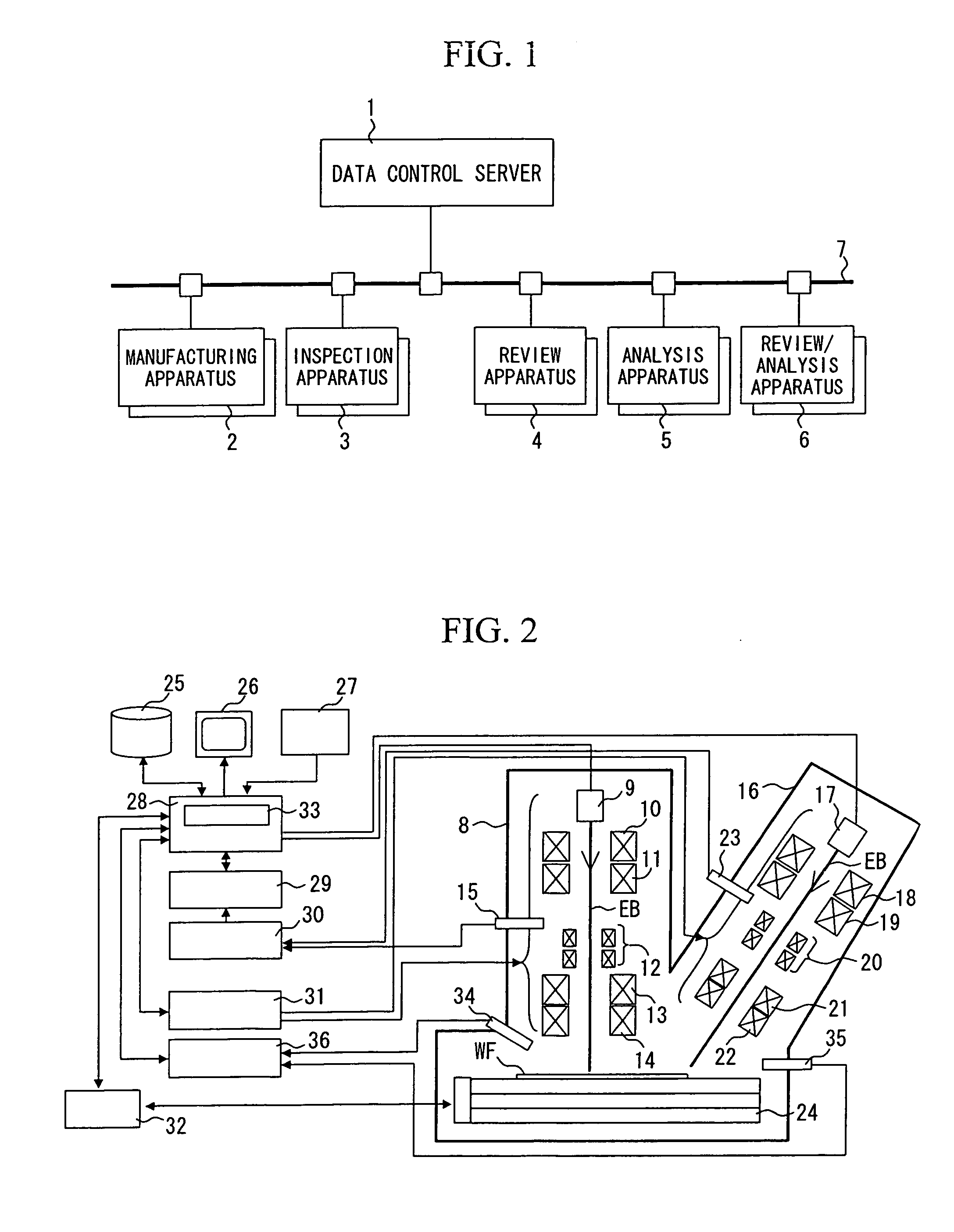
Figure 2 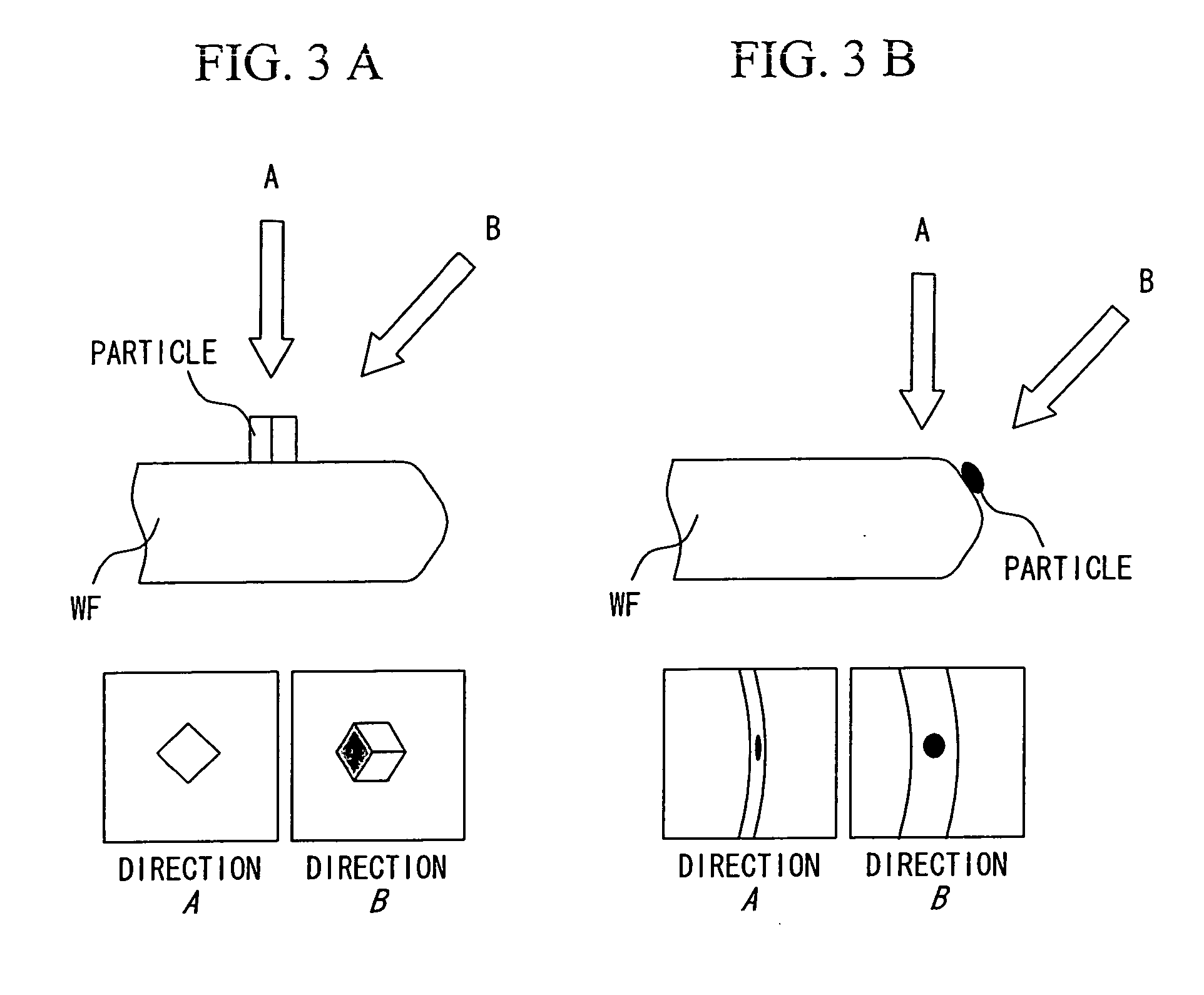
Figure 3
Abstract
Description
CLAIM OF PRIORITY
[0001] The present application claims priority from Japanese application JP 2005-352304 filed on Dec. 6, 2005, the content of which is hereby incorporated by reference into this application.BACKGROUND OF THE INVENTION
[0002] 1. Field of the Invention
[0003] The present invention relates to a method and an apparatus for reviewing defects that have occurred in processes of manufacturing thin film devices such as semiconductor electronic circuit substrates and liquid crystal display substrates, by using a magnification image-pickup apparatus such as a scanning electron microscope.
[0004] 2. Description of the Related Art
[0005] Manufacturing of thin film devices, such as semiconductors, liquid crystal displays, and magnetic heads for hard disks, includes a large number of processes. The number of such manufacturing processes sometimes sums to several hundreds. In a case where defects such as particles and breaks in wiring occur in thin film devices due to unsatisfactory or malf...
Examples
Embodiment Construction
[0028]An embodiment of the present invention is described below by referring to the accompanying drawings.
[0029]By using FIG. 1, descriptions will be given, as a specific example, of each of apparatuses on a wafer manufacturing line and a connection configuration thereof. In FIG. 1, reference numeral 1 denotes a data control server; reference numeral 2, a semiconductor manufacturing apparatus; reference numeral 3, an inspection apparatus; reference numeral 4, a review apparatus; reference numeral 5, an analysis apparatus; reference numeral 6, a review / analysis apparatus; and reference numeral 7, a network. As shown in FIG. 1, the manufacturing line has a configuration in which the semiconductor wafer manufacturing apparatus 2, the inspection apparatus 3, the review apparatus 4, the analysis apparatus 5 and the review / analysis apparatus 6 are connected to one another via the data control server 1 and the network 7.
[0030]The manufacturing apparatus 2 has a function as a lithography ma...