
Opto-electronic device assembly
Patent Information
- Authority / Receiving Office
- US · United States
- Current Assignee / Owner
- Publication Date
- 2013-10-10
- Estimated Expiration
- Not applicable · inactive patent
Smart Images
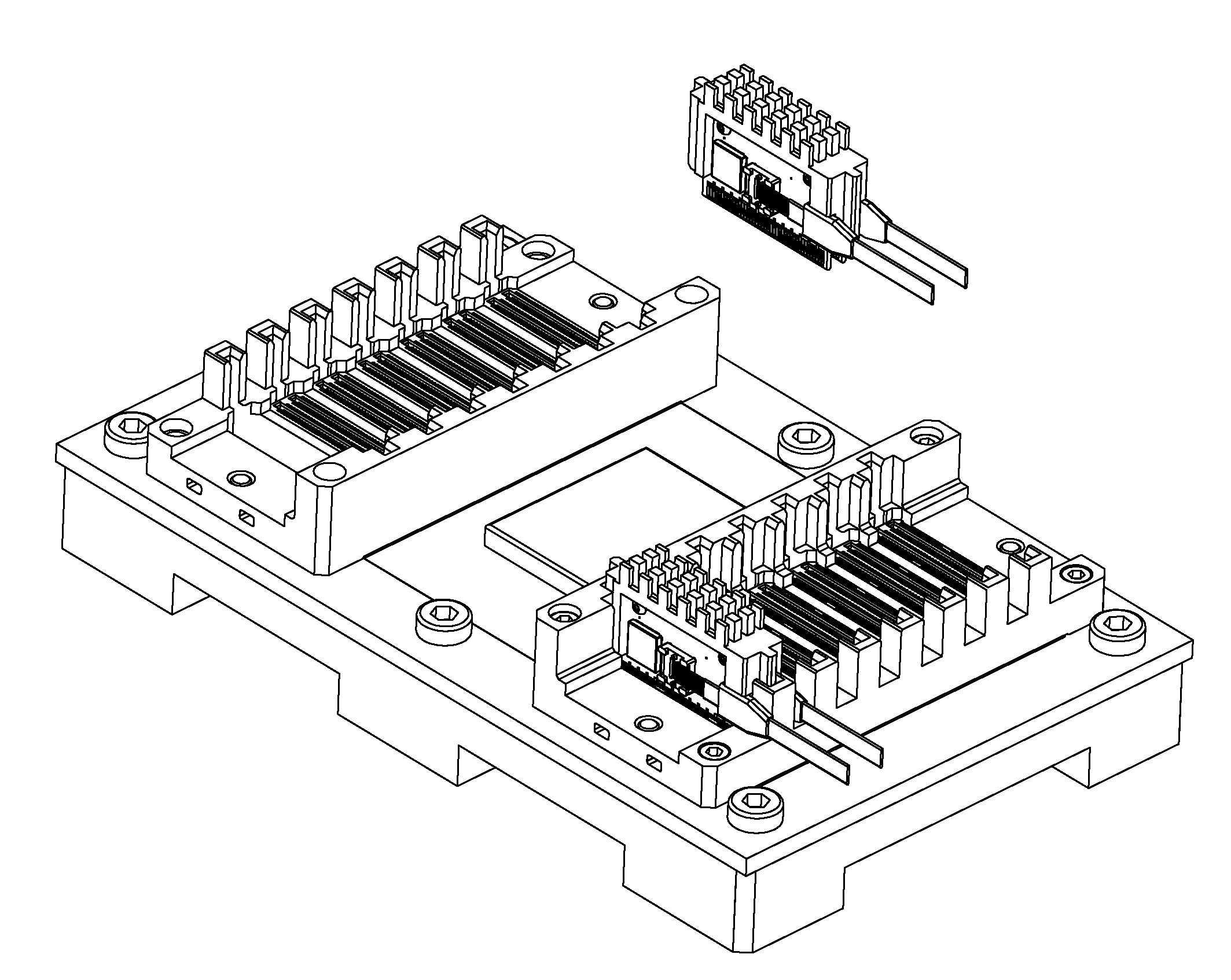
Figure 1 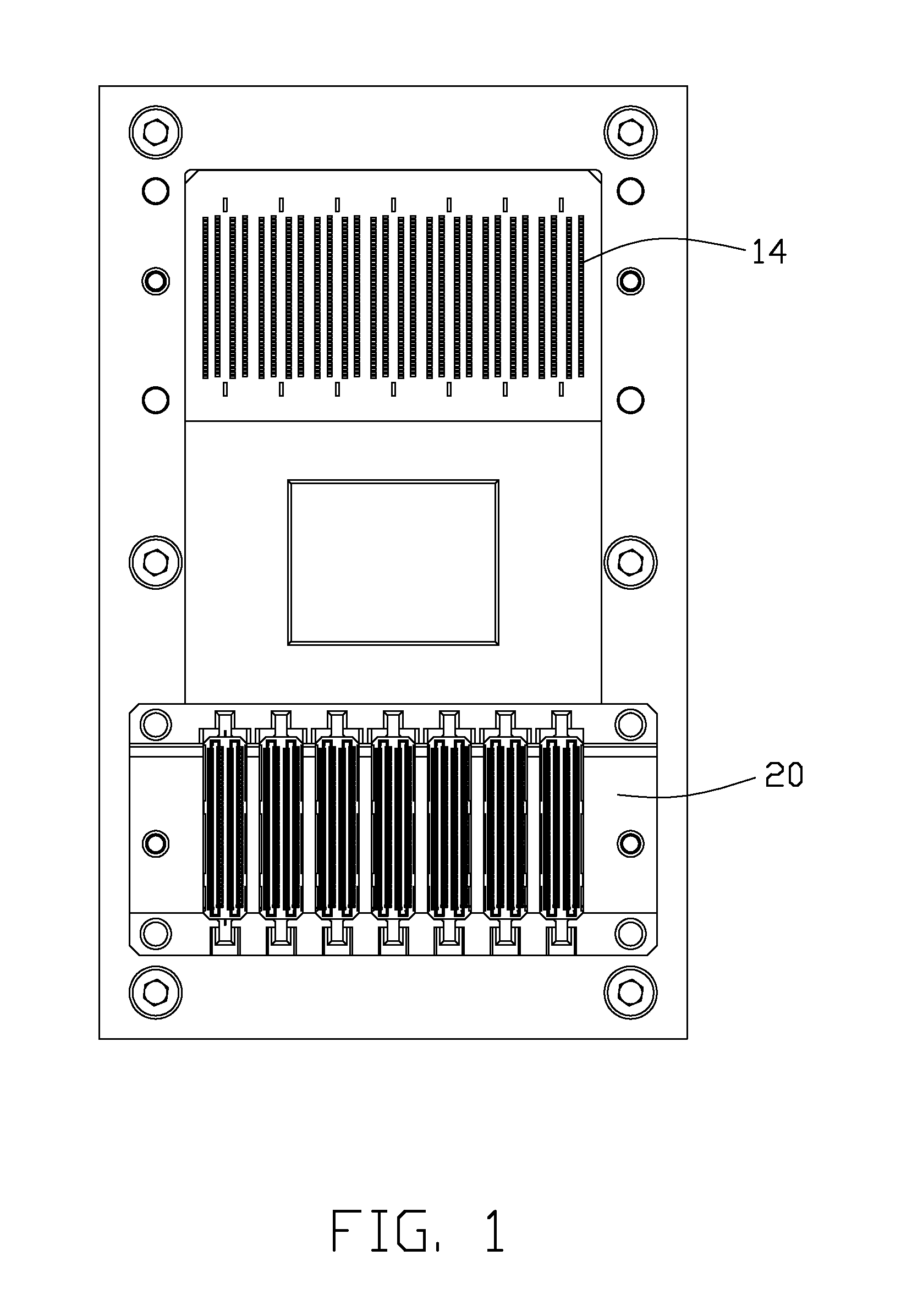
Figure 2 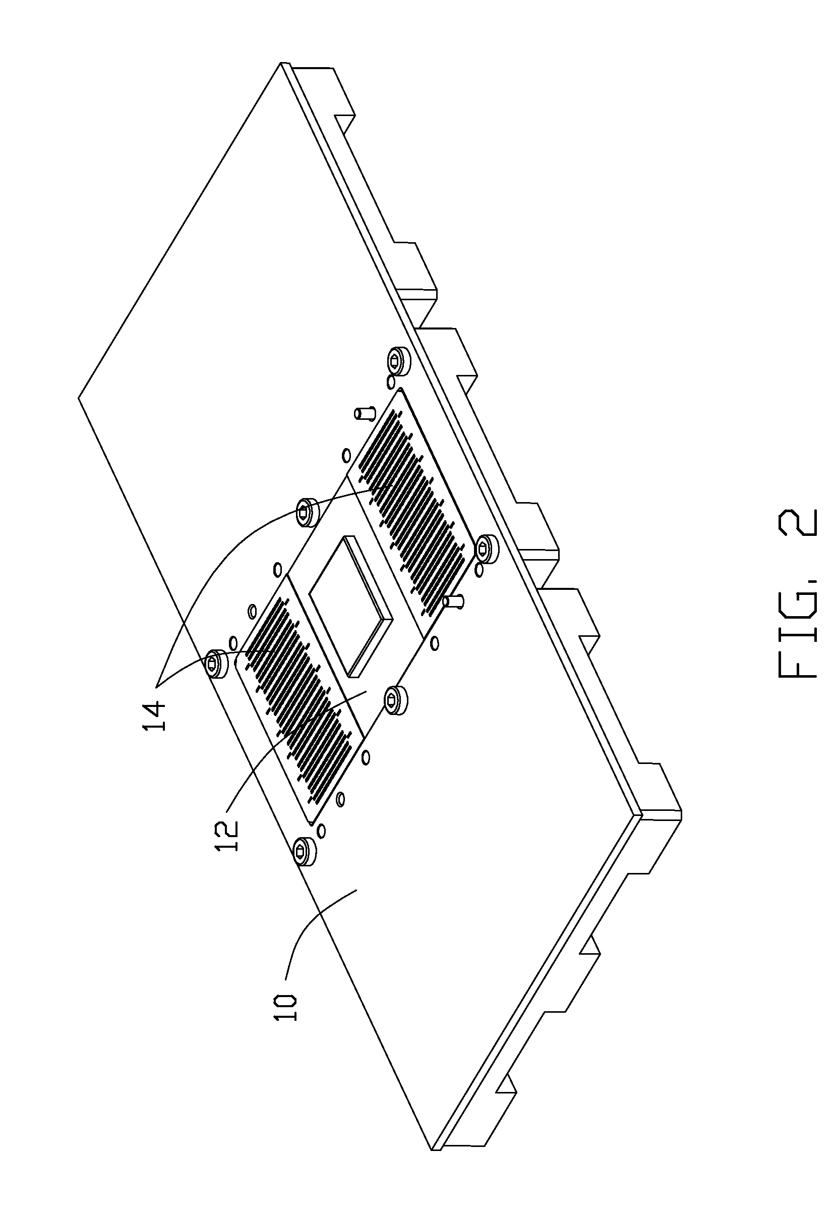
Figure 3
Abstract
Description
BACKGROUND OF THE INVENTION
[0001] 1. Field of the Invention
[0002] The present invention relates to opto-electronic (OE) device assemblies, and more specifically to integrating multiple OE modules with waveguide, e.g., Fiber or Polymer Waveguide (PWG), as an OE sub-assembly to further reduce user's installation and testing costs.
[0003] 2. Description of Related Art
[0004] Most computer and communication networks today rely on copper wire to transmit data between nodes in the network. Since the data transmitted over the copper wire and the data processed within the nodes are both represented in the form of electrical signals, the transfer of data at the node-copper wire interface is straight forward. Other than perhaps level shifts and signal amplification, no other signal processing is required for data transmitted over the copper wire to be decoded by the node. The drawback with using copper wire is its relatively narrower bandwidth. Copper's ability to transmit data is significantly lim...
Examples
Embodiment Construction
[0039]Reference will now be made in detail to the preferred embodiment of the present invention.
[0040]Referring FIGS. 1-24, an aluminum frame 10 defines a ceramic substrate receiving area to receive a ceramic substrate 12 therein. The ceramic substrate 12 defines two connector areas 14, on two opposite ends in a longitudinal direction, forming LGA (Land Grid Array) pads 16 thereon. A modular SLC (Surface Laminar Circuit) interconnect system 18 is fastened to the aluminum frame 10 around each of the connector areas 14, and includes an aluminum organizer 20 defining a plurality of elongated cavities 22 in a transverse direction perpendicular to the longitudinal direction while each of the cavities 22 extends along the longitudinal direction. The aluminum organizer 20 defines a plurality of fastening holes 24 and a plurality of locating holes 26 to receive corresponding screws 28 and dowel pins 30 for locating and fastening the organizer 20 upon the aluminum frame 10. The organizer 20 ...