
High voltage integrated circuit device
a high-voltage integrated circuit and integrated circuit technology, applied in the field of high-voltage integrated circuit devices, can solve problems such as malfunction and destruction of /b>, and achieve the effects of preventing false signal transmission of high-side logic, and preventing the implantation of excessive hole curren
Patent Information
- Authority / Receiving Office
- US · United States
- Patent Type
- Applications(United States)
- Current Assignee / Owner
- Publication Date
- 2015-08-20
Smart Images
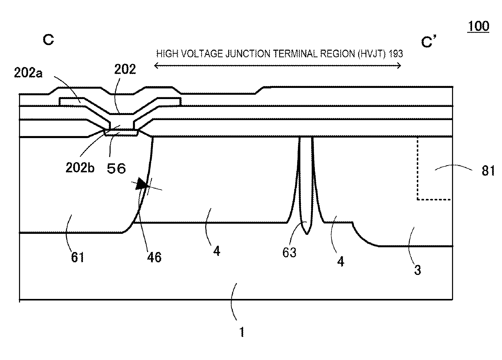
Figure 1 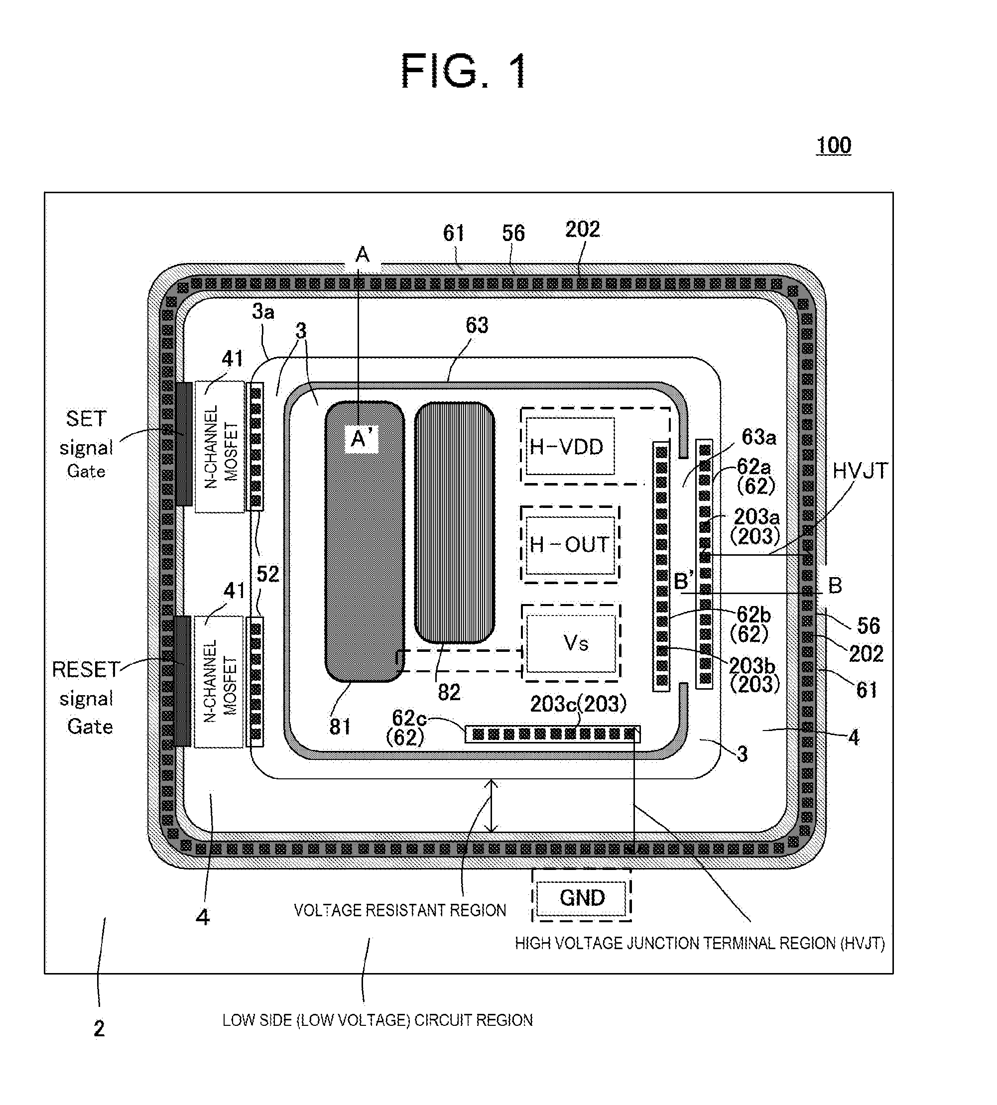
Figure 2 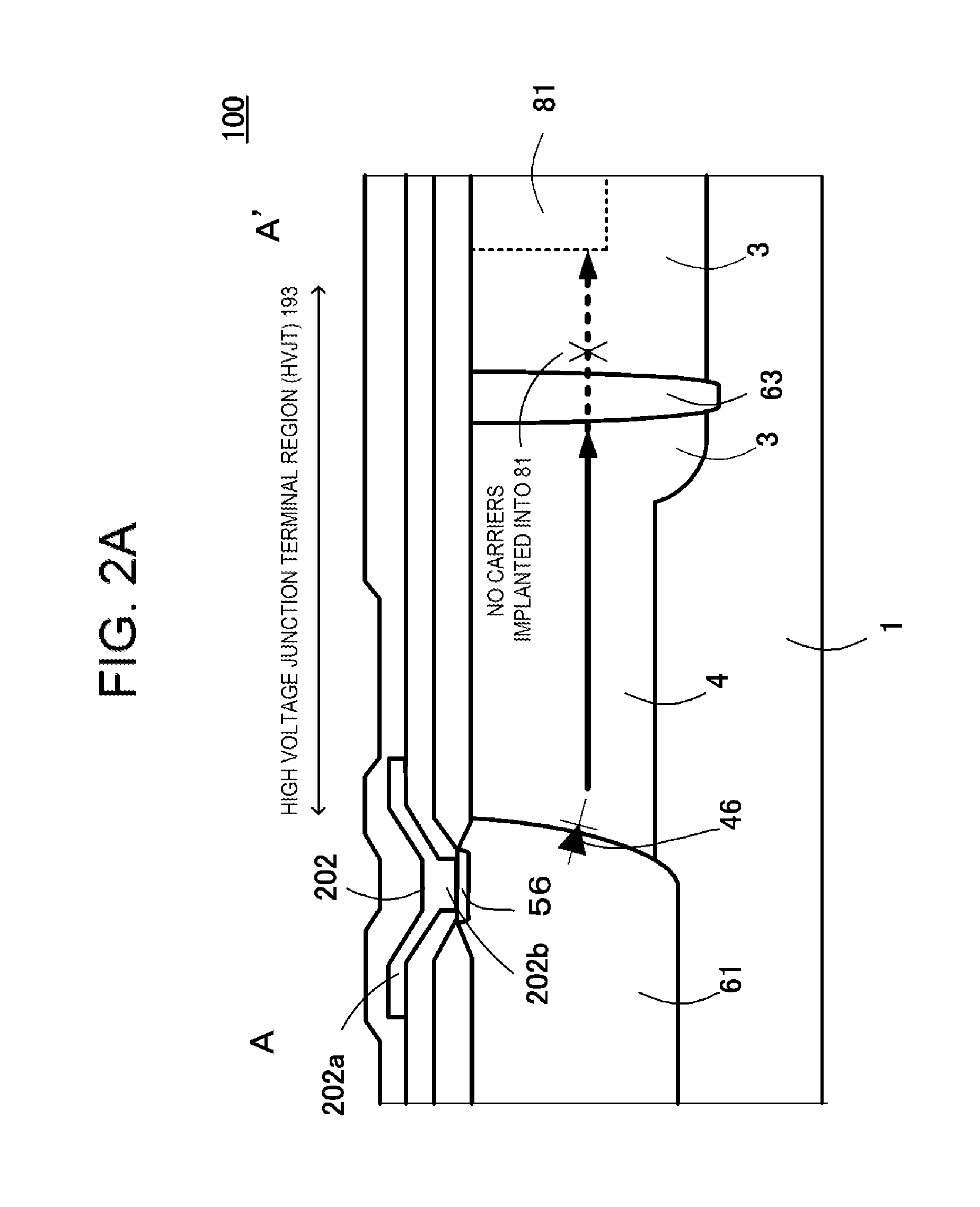
Figure 3
Abstract
Description
CROSS-REFERENCE TO RELATED APPLICATIONS
[0001] This application claims the benefit of foreign priority of Japanese patent applications 2014−029679, filed Feb. 19, 2014, and 2015−000615, filed Jan. 6, 2015. The disclosures of these Japanese priority applications are incorporated herein by reference.BACKGROUND OF THE INVENTION
[0002] 1. Field of the Invention
[0003] The present invention relates to a high voltage integrated circuit device (HVIC). In particular, the invention relates to a high voltage integrated circuit device such that malfunction due to an overcurrent flowing when a negative voltage surge is input into a circuit is prevented from occurring.
[0004] 2. Description of the Background Art
[0005] An element isolation type of HVIC that utilizes a high breakdown voltage junction is used in a method of driving a switching power device configuring the upper arm of a power conversion (direct current to alternating current conversion) bridge circuit such as a PWM inverter. The HVIC has in...
Examples
embodiment 1
[0076]FIGS. 1 and 2A and 2B are configuration diagrams of a high voltage integrated circuit device 100 of a first embodiment according to the invention, FIG. 1 being a main portion plan view and FIGS. 2A and 2B being main portion sectional views of FIG. 1, wherein FIG. 2A is a main portion sectional view cut along an A-A′ line of FIG. 1, and FIG. 2B is a main portion sectional view cut along a B-B′ line of FIG. 1.
[0077]The high voltage integrated circuit device 100 includes an n-type well region 3, which is a high potential region formed in a surface layer of a p-type substrate 1 (semiconductor layer), and an n−-type well region 4, which is a voltage-resistant region of an impurity concentration lower than that of the n-type well region 3, in contact with the n-type well region 3 in the surface layer of the p-type substrate 1 and formed around the outer periphery of the n-type well region 3.
[0078]Also, the high voltage integrated circuit device 100 includes a p-type common potential...
embodiment 2
[0112]FIG. 4 is a main portion plan view of a high voltage integrated circuit device 200 of a second embodiment of the invention. FIG. 4 differs from FIG. 1 in that the p−-type aperture portion 63 having the gap portion 63a is disposed inside the n−-type well region 4, which is a voltage resistant region, and one second high concentration region 62 is disposed in the end portion of the n-type well region 3, which is a high potential region.
[0113]The width of the p−-type aperture portion 63 is such that breakdown voltage characteristics are not lost even when the H-VDD terminal (pad) leaps to a high potential of in the region of 600V. In order to achieve this, the width of the p−-type aperture portion 63 is set to the width for which depletion layers extending from the n-type well region 3 to the p−-type aperture portion 63 are in contact, so that the p−-type aperture portion 63 is depleted. Herein, the width of the p−-type aperture portion 63 is a width in the region of 10 to 20 μm....
embodiment 3
[0115]FIGS. 13 and 14A and 14B are configuration diagrams of a high voltage integrated circuit device 200a of a third embodiment according to the invention, wherein FIG. 13 is a main portion plan view and FIGS. 14A and 14B are main portion sectional views cut along a C-C′ line and D-D′ line of FIG. 13.
[0116]FIGS. 13 and 14A and 14B differ from FIG. 4 in that the second high concentration region 62 of the n−-type well region 4, which is a voltage resistant region, is formed in the vicinity of the boundary with the n-type well region 3, which is a high potential region. The HVJT 193 in this place is a region formed of the second high concentration region 62, the n−-type well region 4, which is a voltage resistant region, the p-type common potential region 61, and the first high concentration region 56. When an n-type offset region 80 is formed so as to envelop the second high concentration region 62, a drop in breakdown voltage can be suppressed. It is good when the impurity concentra...