
Semiconductor device and semiconductor device manufacturing method
a semiconductor device and semiconductor technology, applied in the direction of semiconductor devices, basic electric elements, electrical appliances, etc., can solve the problems of thermal runaway destruction, high production cost, and high production cost, and achieve the effect of suppressing the implantation of holes, reducing the occurrence of leakage current, and gentle concentration gradien
Patent Information
- Authority / Receiving Office
- US · United States
- Patent Type
- Patents(United States)
- Current Assignee / Owner
- Publication Date
- 2016-04-26
Smart Images
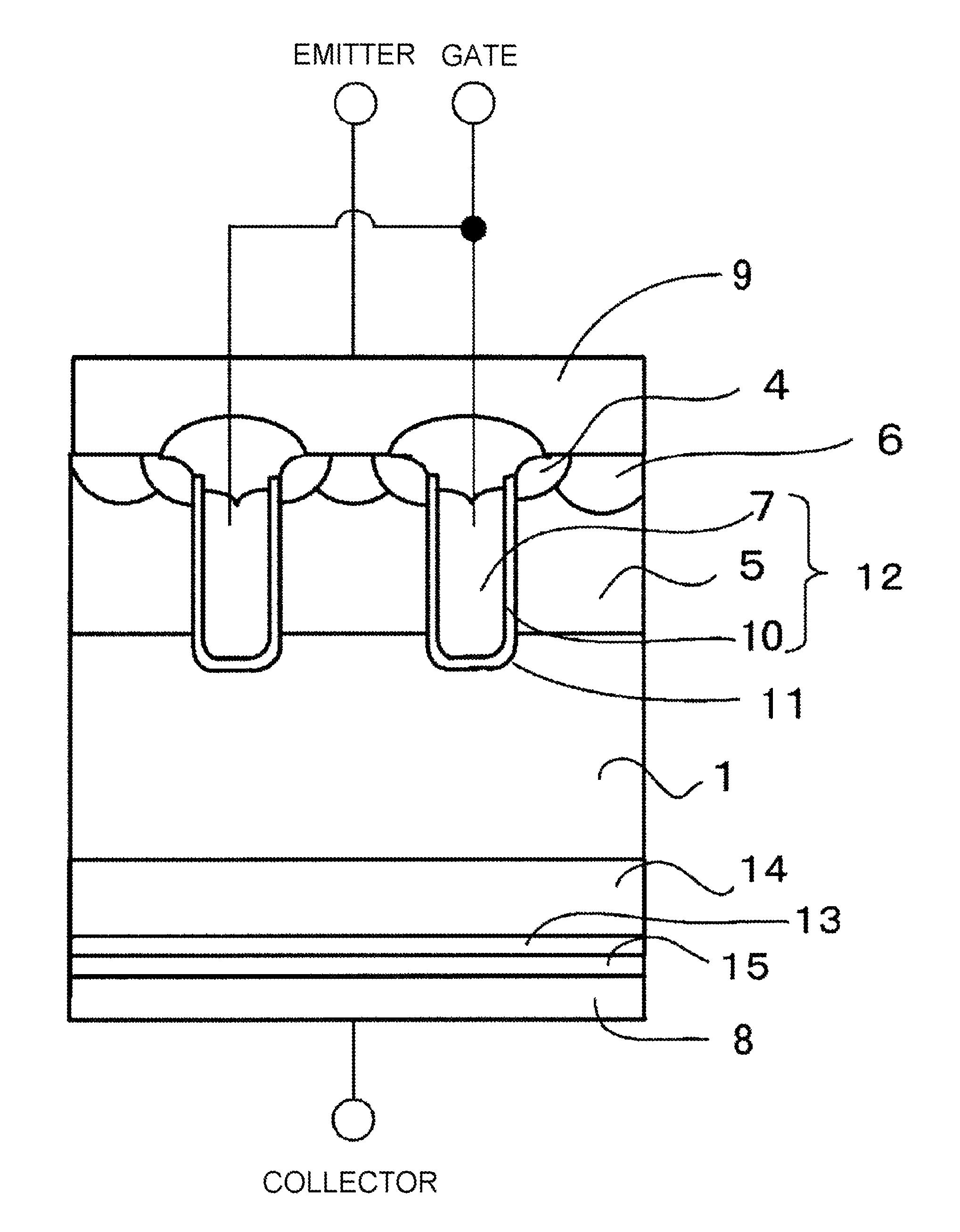
Figure 1 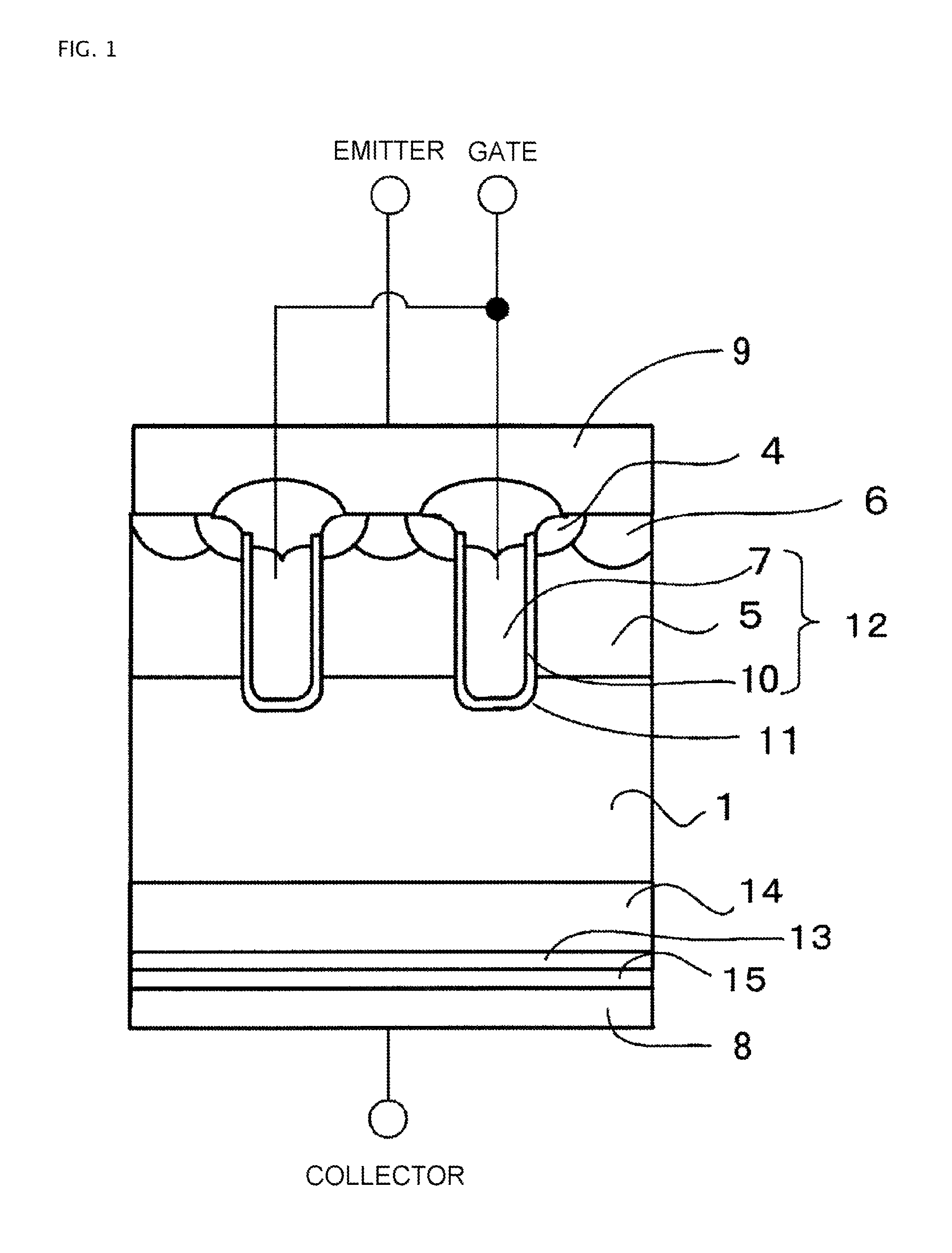
Figure 2 
Figure 3
Abstract
Description
[0001] This application is a continuation of International Application No. PCT / JP2012 / 062875, filed on May 18, 2012, which is based on and claims priority to Japanese Patent Application No. JP PA 2011-111709, filed on May 18, 2011. The disclosure of the Japanese priority application and the PCT application in their entirety, including the drawings, claims, and the specification thereof, are incorporated herein by reference.BACKGROUND
[0002] 1. Field of the Invention
[0003] Embodiments of the invention relate to a semiconductor device and semiconductor device manufacturing method, and in particular, relate to a semiconductor device and semiconductor device manufacturing method such that a field-stop layer is provided on a substrate back surface side.
[0004] 2. Related Art
[0005] An IGBT (Insulated Gate Bipolar Transistor) is a power element wherein the high speed switching characteristics and voltage drive characteristics of a MOSFET (Metal-Oxide-Semiconductor Field Effect Transistor) and the...
Examples
embodiment
[0034]A field-stop IGBT (FS-IGBT) according to an embodiment of the invention will be described in detail with reference to FIGS. 1, 6 and the like, with a trench-FS-IGBT with a breakdown voltage of, for example, 1,700V as an example. FIG. 1 is a main portion sectional view showing the configuration of the FS-IGBT according to the embodiment of the invention. FIG. 6 is a characteristic diagram showing the impurity concentration distribution of the FS-IGBT according to the embodiment of the invention. FIG. 6 shows the impurity concentration distribution from the back surface to an n− type drift layer 1 of a silicon (Si) substrate (semiconductor substrate) configuring the trench-FS-IGBT (the same also applies to FIG. 7).
[0035]The trench-FS-IGBT shown in FIG. 1 is configured using, for example, an FZ-n-type Si substrate formed of an inexpensive FZ wafer. The resistivity of the Si substrate may be in the region of, for example, 80 Ωcm to 130 Ωcm. The thickness of the finished Si substra...