
Semiconductor die adapter and method of using
a technology of silicon die and adapter, which is applied in the direction of individual semiconductor device testing, semiconductor/solid-state device testing/measurement, instruments, etc., can solve the problems of low yield of functioning mcm's, low efficiency of mcm's, and high percentage of chips on a wafer that function properly, etc., to achieve less damage, greater surface area, and more robust
Patent Information
- Authority / Receiving Office
- US · United States
- Patent Type
- Patents(United States)
- Current Assignee / Owner
- Publication Date
- 2005-04-19
- Estimated Expiration
- Not applicable · inactive patent
Smart Images
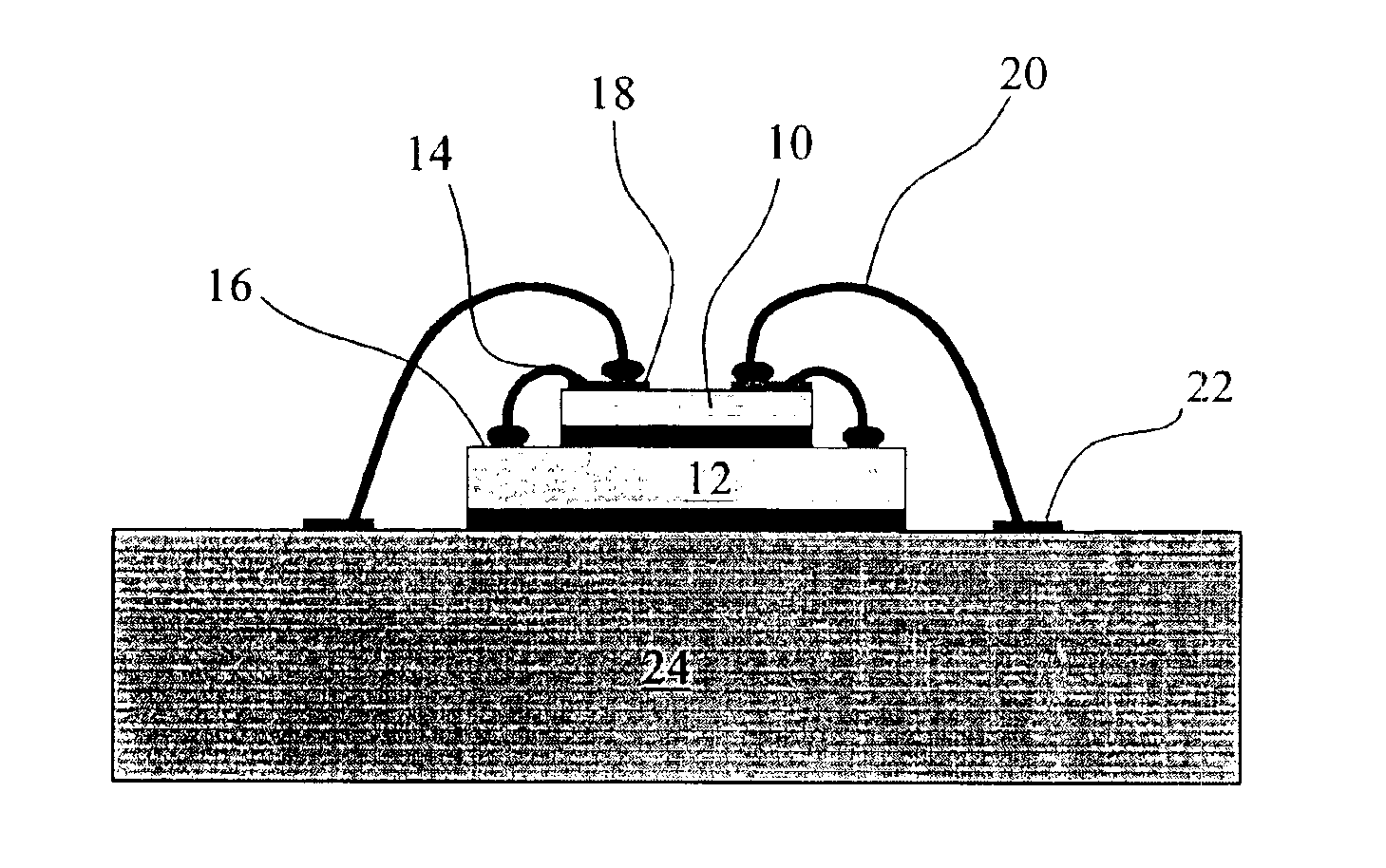
Figure 1 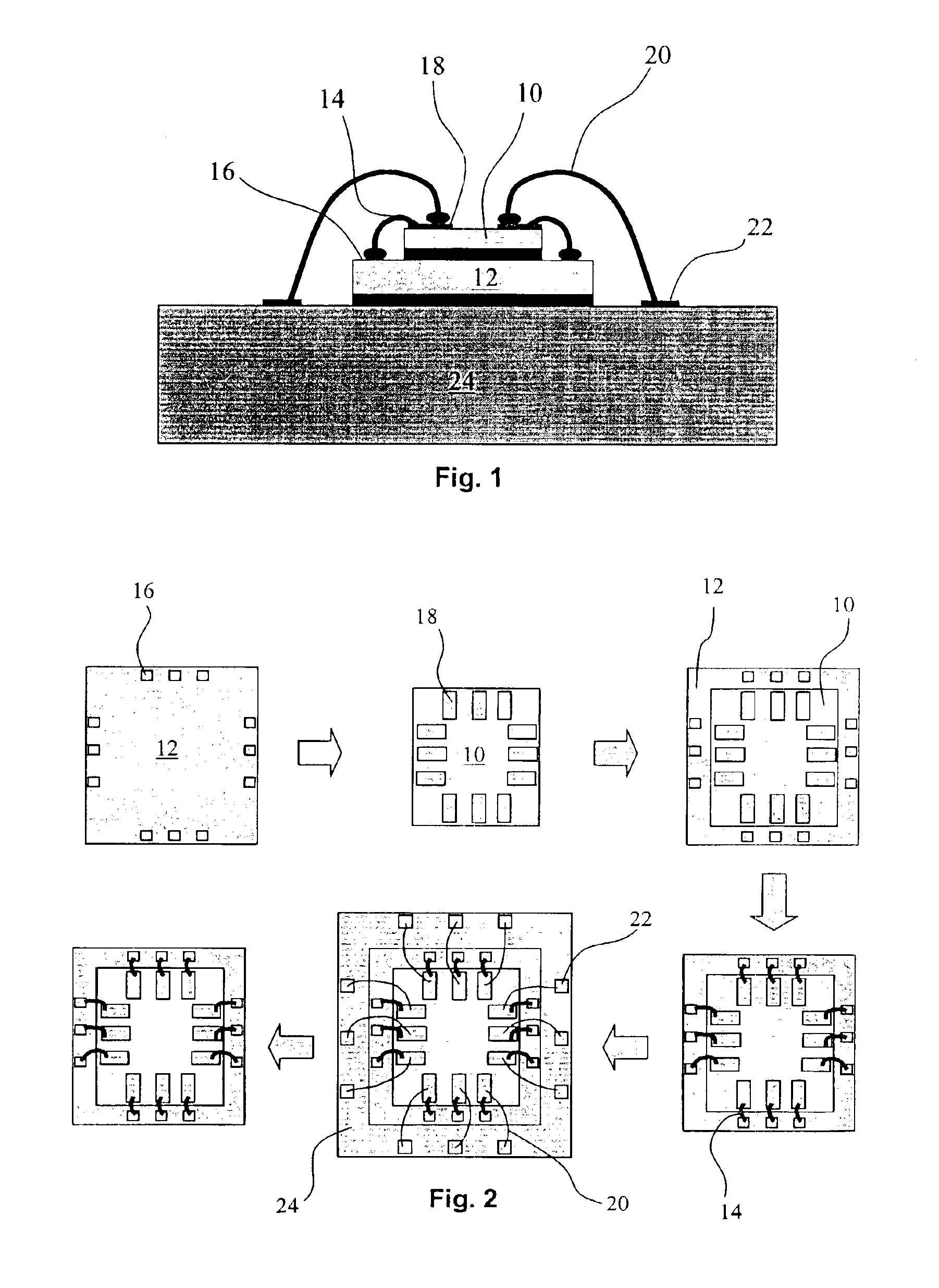
Figure 2 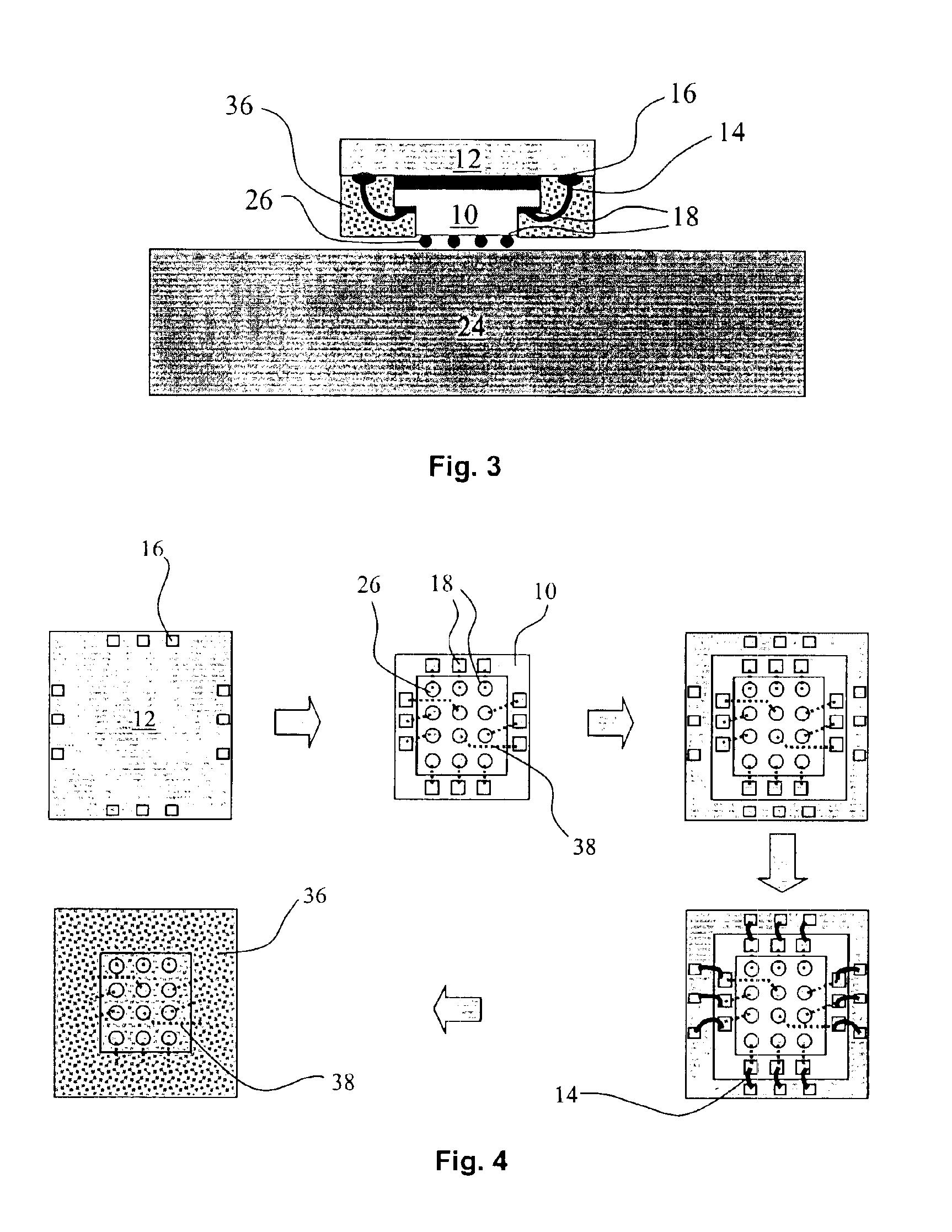
Figure 3
Abstract
Description
CROSS-REFERENCE TO RELATED APPLICATION
[0001] This application claims the benefit of the co-pending U.S. Provisional Application No. 60 / 294,737, filed on May 31, 2001.BACKGROUND OF THE INVENTION
[0002] 1. Field of the Invention
[0003] The present invention relates to an apparatus and method for reliably testing and installing individual integrated circuit chips using die adapters that minimize damage to the chips.
[0004] 2. Description of the Related Art
[0005] A semiconductor die (plural “dice”) is an integrated circuit designed to serve a specific function, such as a memory chip, in an electronic device. Dice are generally fabricated together in rows on a silicon wafer. During die fabrication, also known as wafer processing, photolithography is traditionally used to first print an image of the micro-circuitry of each die on a wafer surface, duplicating the circuit image at each adjacent die location until the wafer surface is filled. Subsequent processing often including ion implantation, e...
Examples
first embodiment
[0020]the present invention is illustrated in FIG. 1. It includes an adapter 10 that is bonded to the active side of an integrated circuit die 12. Die-to-adapter connectors 14 connect die bond pads 16 to corresponding adapter bond pads 18. Finally, adapter-to-substrate connectors 20 connect the adapter bond pads 18 to device contacts 22 on a device substrate 24 such as a printed circuit board or module.
[0021]A significant feature of the present invention teaches that the adapter 10 may be permanently bonded to the die 12 so that the adapter 10 may accompany the die 12 through testing in a temporary package and into final assembly in a device or module. That means that the die-to-adapter connectors 14 are bonded to the die bond pads 16 only once. The adapter bond pads 18 may be designed to be larger and more robust than the corresponding die bond pads 16. Increasing bond pad surface area on the adapter 10 results in more reliable bonds. Also, because connections to the relatively fra...
second embodiment
[0027]FIG. 3 illustrates the present invention involving a flip chip. Here the adapter 10 and the die 12 are turned upside down and the active surface of the die 12 faces the substrate. The die-to-adapter connectors 14 may again comprise wire bonds; however the adapter-to-substrate connectors 20 may comprise, instead of wire bonds, reflowed solder bumps 26 connected to the underside of the adapter 10. The solder bumps 26, another source of frequent defects and shorts in traditional integrated circuit packages, are attached to the more robust adapter bond pads 18. A polymer encapsulant 36 may be added around the base of the die 12 to protect the electrical connections.
[0028]FIG. 4 is a process flow diagram illustrating bottom views of the embodiment shown in FIG. 3 during various stages of fabrication. Starting with a bare flip chip die 12 shown in the upper left hand corner of FIG. 4, the adapter 10 is bonded to the die 12 and wire bonds are used as the die to adapter electrical con...