
Automatic center frequency tuning of a voltage controlled oscillator
Patent Information
- Authority / Receiving Office
- US · United States
- Current Assignee / Owner
- Publication Date
- 2006-05-02
Smart Images
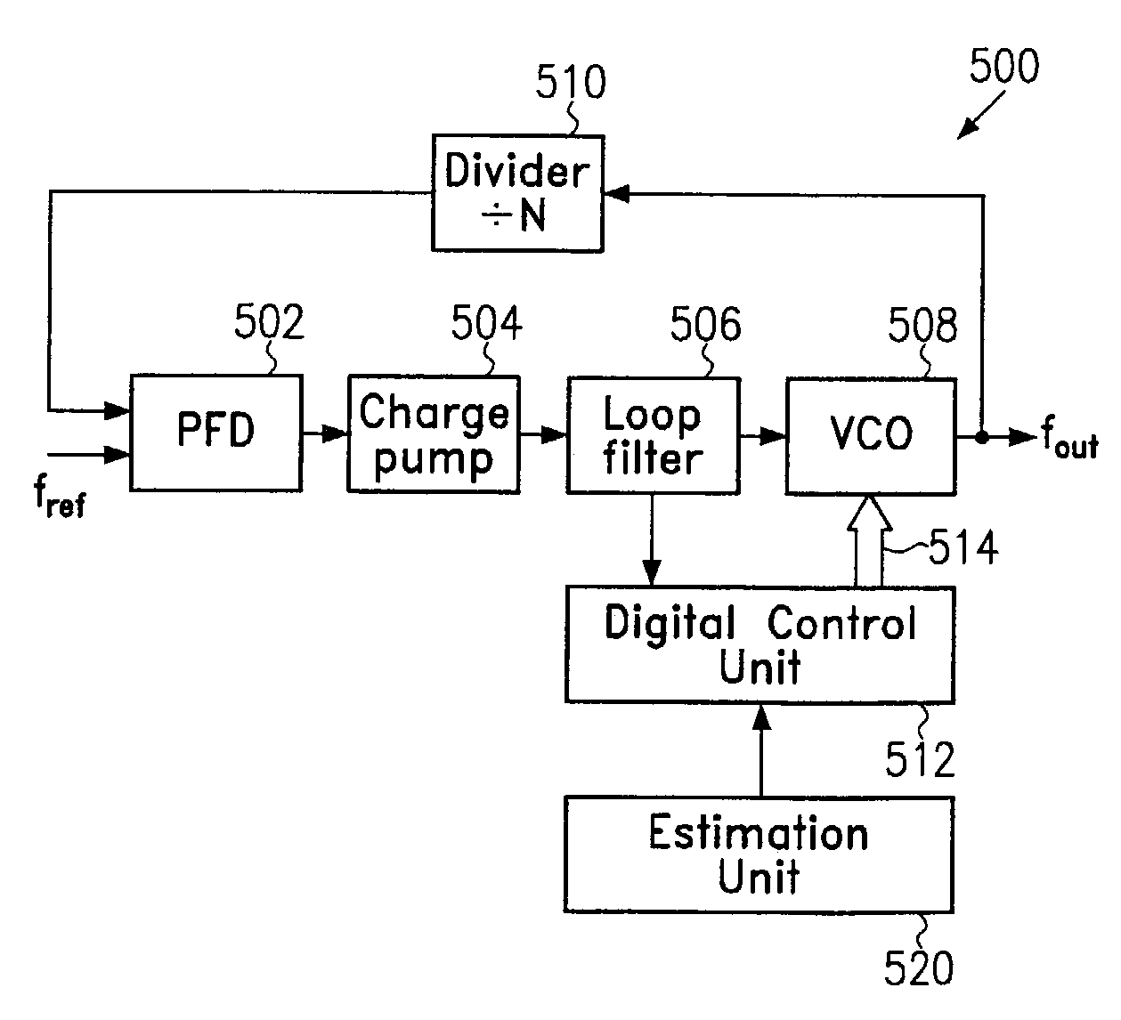
Figure 1 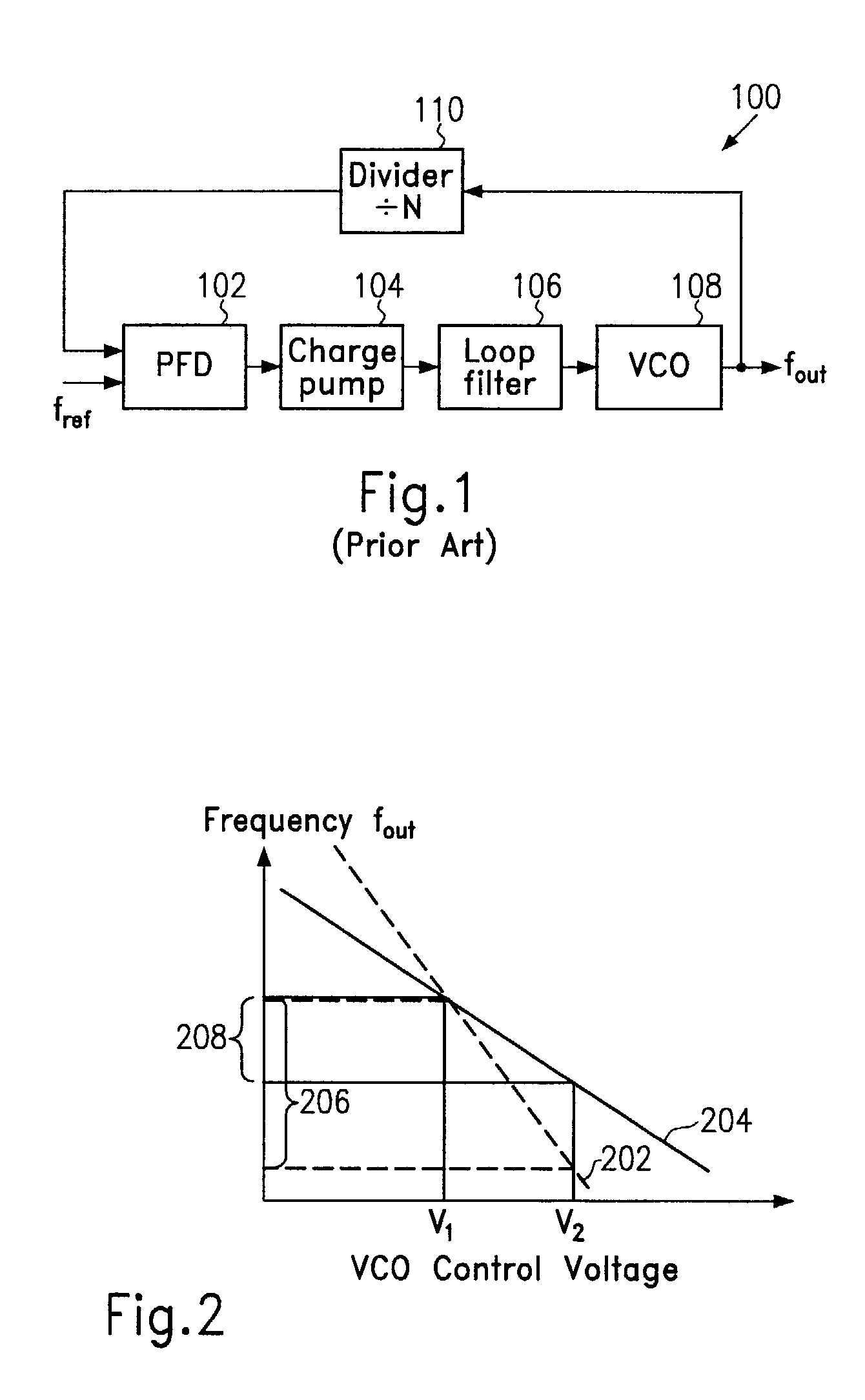
Figure 2 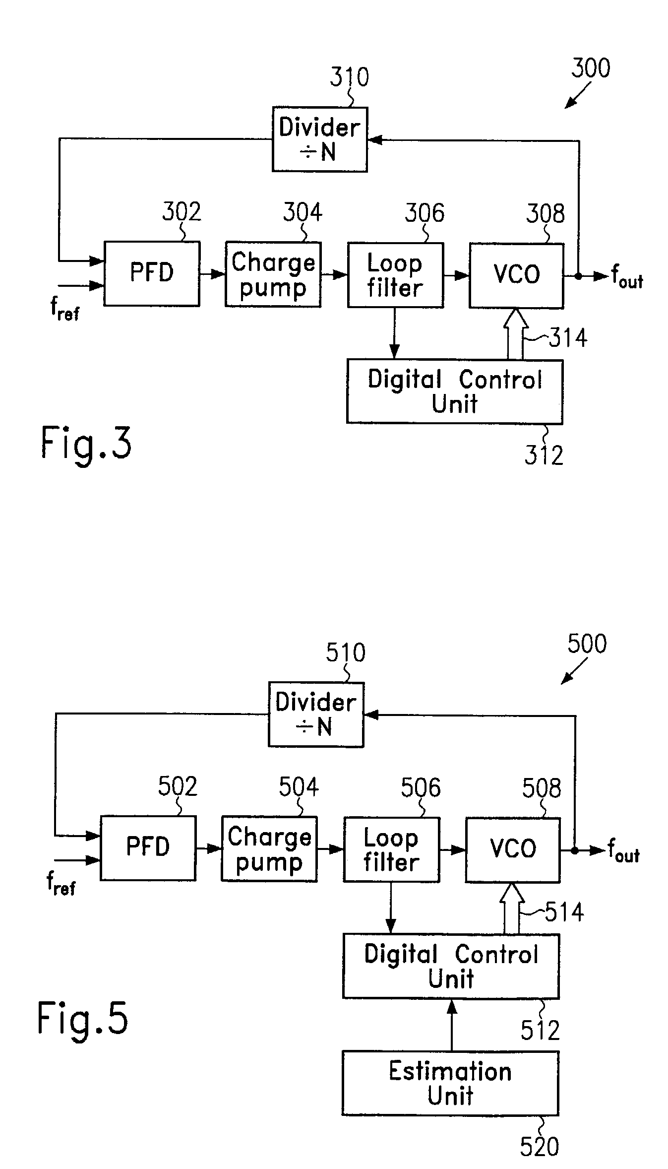
Figure 3
Abstract
Description
BACKGROUND OF THE INVENTION
[0001] 1. Field of the Invention
[0002] The present invention relates generally to the synthesis of high frequency signals. More particularly, the present invention relates to the synthesis of high frequency local oscillator signals for wireless communication applications.
[0003] 2. Description of the Related Art
[0004] Wireless communication systems typically require frequency synthesis in both the received path circuitry and the transmit path circuitry. Phase locked loop (PLL) circuits including voltage control oscillators (VCO) are of use in mobile unit applications to produce a desired output frequency fout. As depicted in FIG. 1, a typical PLL circuitry 100 uses a phase / frequency detector 102 for detecting a frequency and / or phase difference between a reference frequency fref and the divided output frequency to drive a charge pump 104. This charge pump 104 delivers packets of charge proportional to the phase difference and / or frequency difference to a loop f...
Examples
Embodiment Construction
[0023]The illustrated embodiments of the present invention will be described with reference to the figure drawings, wherein like elements and structures are indicated by a like reference numbers.
[0024]Referring now to the drawings and in particular to FIG. 3, which is a block diagram of a frequency synthesizer usable in a wireless communication device according to one embodiment, the frequency synthesizer has a phase locked loop 300 comprising a voltage control oscillator 308 for generating an output signal having an output frequency fout. The output signal is frequency divided by means of a divider 310, which may be an integer N divider. This frequency divided signal is compared to a reference signal having a reference frequency fref by means of a phase / frequency detector 302. The phase / frequency detector 302 outputs an error signal, which may be a charge up or charge down and is input to a charge pump 304. The charge pump 304 converts the charge up and charge down signals into a c...