

Non-volatile memory and fabricating method thereof
a non-volatile memory and fabricating method technology, applied in the field of semiconductor devices, can solve the problems of affecting the ultimate reliability of the device and the performance of the device, and achieve the effects of preventing any adverse effects on device performance, reducing line resistance in the source/drain region, and improving short channel
Patent Information
- Authority / Receiving Office
- US · United States
- Patent Type
- Patents(United States)
- Current Assignee / Owner
- Publication Date
- 2006-09-05
Smart Images
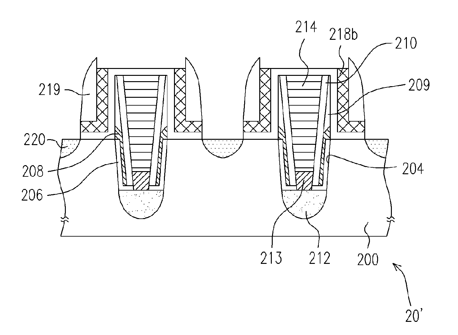
Figure 1 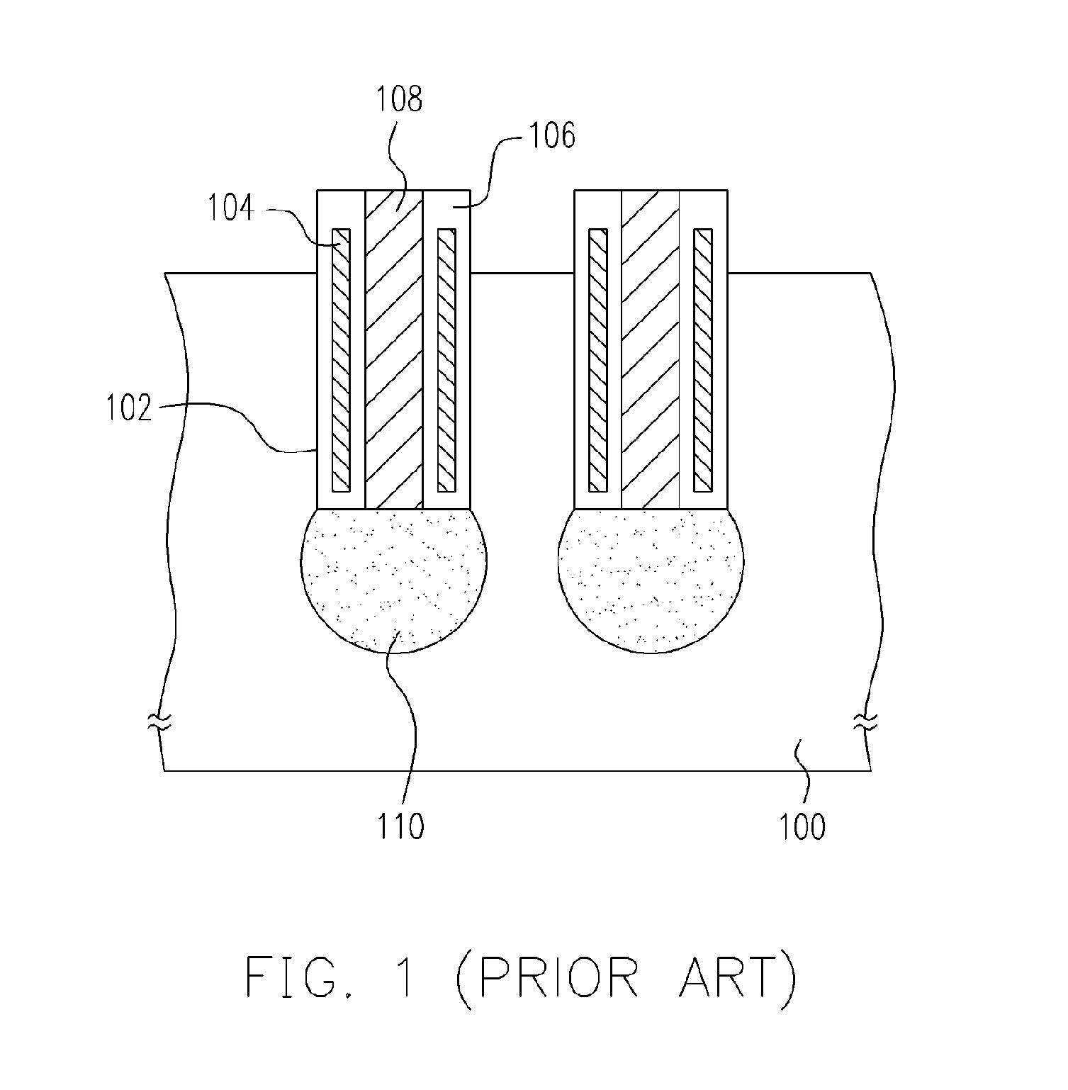
Figure 2 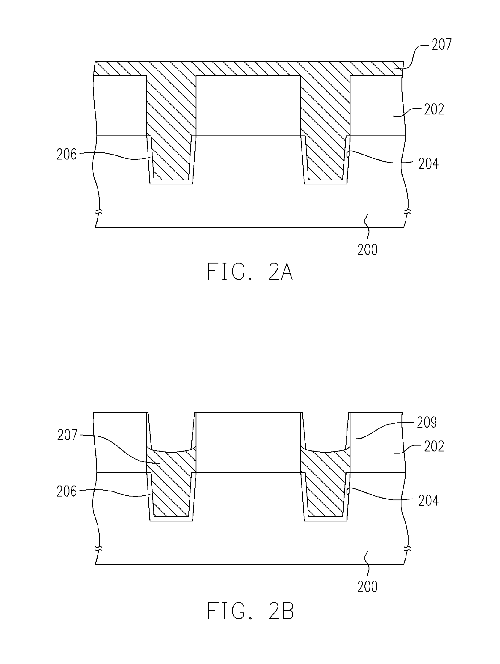
Figure 3
Abstract
Description
CROSS-REFERENCE TO RELATED APPLICATION
[0001] This application claims the priority benefit of Taiwan application serial no. 94120135, filed on Jun. 17, 2005. All disclosure of the Taiwan application is incorporated herein by reference.BACKGROUND OF THE INVENTION
[0002] 1. Field of the Invention
[0003] The present invention relates to a semiconductor device and a fabricating method thereof. More particularly, the present invention relates to a non-volatile memory and a fabricating method thereof.
[0004] 2. Description of the Related Art
[0005] Memory is a semiconductor device designed to store data or parameters. With the production of increasingly powerful microprocessors, the size of the software programs that are operated by memory increases correspondingly. As a result, the demand for a high storage capacity memory is getting higher and higher. The challenge of producing memory with a larger storage capacitor in accordance with this trend is now the force driving the techniques and process...
Examples
Embodiment Construction
[0037]Reference will now be made in detail to the present preferred embodiments of the invention, examples of which are illustrated in the accompanying drawings. Wherever possible, the same reference numbers are used in the drawings and the description to refer to the same or like parts.
[0038]FIGS. 2A through 2G are schematic cross-sectional views showing the steps for fabricating a non-volatile memory according to one embodiment of the present invention. First, as shown in FIG. 2A, a substrate 200 is provided. Then, a patterned mask layer 202 is formed over the substrate 200. The patterned mask layer 202 is fabricated using silicon nitride, for example. Thereafter, using the patterned mask layer 202 as a mask, an etching operation is carried out to form a trench 204 in the substrate 200. A dielectric layer 206, serving as a tunneling oxide layer, is formed on the surface of the trench 204. The dielectric layer 206 is fabricated using silicon oxide, for example. The dielectric layer...