
Method for manufacturing metal-oxide-semiconductor transistor
An oxide semiconductor and transistor technology, applied in semiconductor/solid-state device manufacturing, electrical components, circuits, etc., can solve problems such as unsatisfactory lateral diffusion of P-type dopants, and achieve improved short-channel effects and good junction profiles. Effect
Patent Information
- Authority / Receiving Office
- CN · China
- Patent Type
- Applications(China)
- Current Assignee / Owner
- Publication Date
- 2008-05-14
Smart Images
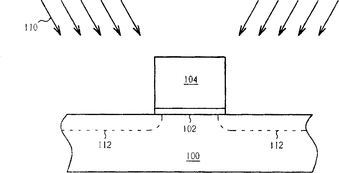
Figure 1 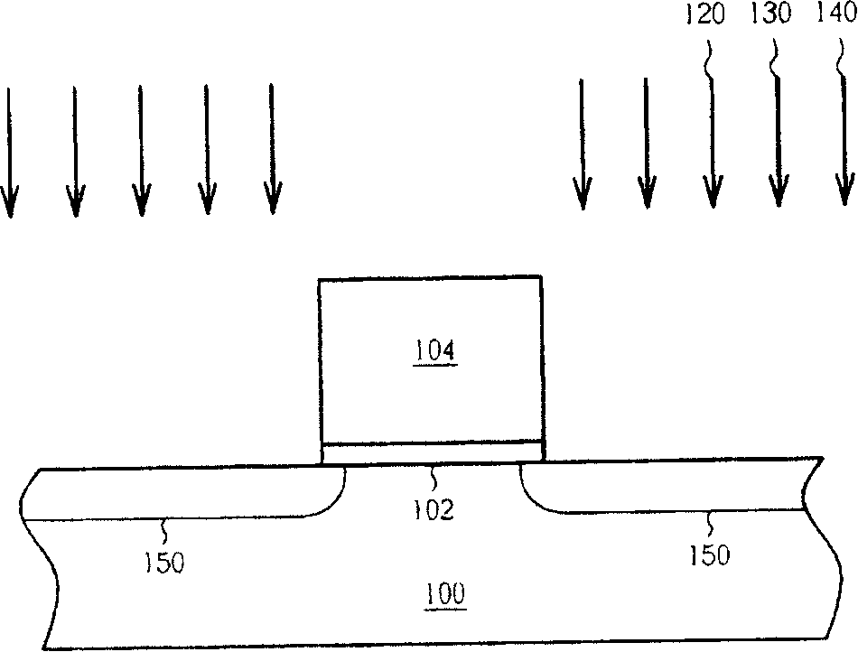
Figure 2 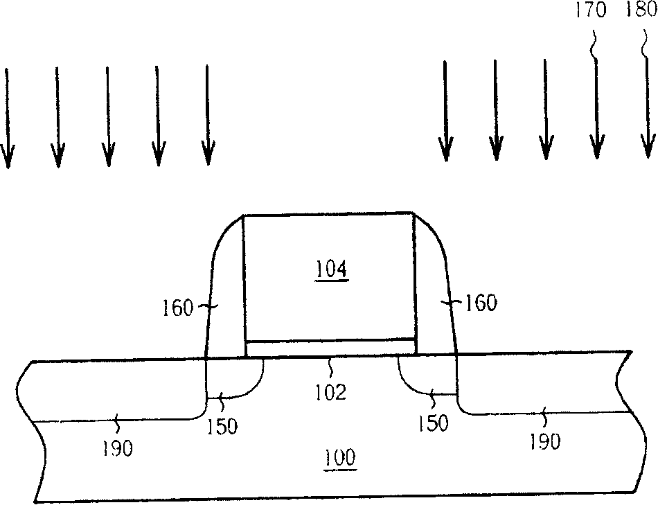
Figure 3
Abstract
Description
technical field
[0001] The present invention relates to a method for manufacturing a metal-oxide semiconductor (hereinafter referred to as MOS) transistor, in particular to a method that can effectively improve the transient enhanced diffusion (hereinafter referred to as TED) effect and short channel Effect (short channel effect) method of manufacturing MOS transistors. Background technique
[0002] With the advancement of process technology and the requirements for high speed and low power consumption of logic elements, the size of MOS transistors has also been shrunk down to the miniaturization size below the micron or nanometer level, and the short channel effect is accompanied by the scaling of MOS transistors. , and the resulting drop in transistor start voltage, the industry generally overcomes it by fabricating a lightly doped drain (LDD) with an ultra shallow junction.
[0003] The existing ultra-shallow junction formation technology is to implant low-energy ions on...
Examples
Embodiment Construction
[0043] see Figure 4 to Figure 8 , Figure 4 to Figure 8 It is a schematic diagram of the first preferred embodiment of the method for manufacturing a MOS transistor provided by the present invention. Such as Figure 4 As shown, a substrate 200 is firstly provided. The substrate 200 can be a semiconductor wafer, a silicon-on-insulator (SOI wafer), etc. The substrate 200 has completed the shallow trench isolation (STI) process and the doping of the well (well). complex process, and a gate structure 210 at least composed of a gate dielectric layer 212 and a gate 214 has been formed on the substrate 200 . Then, a pre-amorphization (PAI) process 220 is performed. The PAI process 220 can be a right-angle or angled PAI process to form an amorphized region 222 in the substrate 200 on both sides of the gate structure 210. .
[0044] see Figure 5 . Next, a co-implantation process 230 is performed to implant a co-implantation dopant 232 into the amorphized region 222 . It should...