
Pixel defect correction device
a defect correction and pixel technology, applied in the field of pixel defect correction devices, can solve the problems of reducing the size of the photodiode and the v transfer path increasing the probability of defect generation, white flaw, and black flaw
Patent Information
- Authority / Receiving Office
- US · United States
- Patent Type
- Patents(United States)
- Current Assignee / Owner
- Publication Date
- 2009-09-22
- Estimated Expiration
- Not applicable · inactive patent
Smart Images
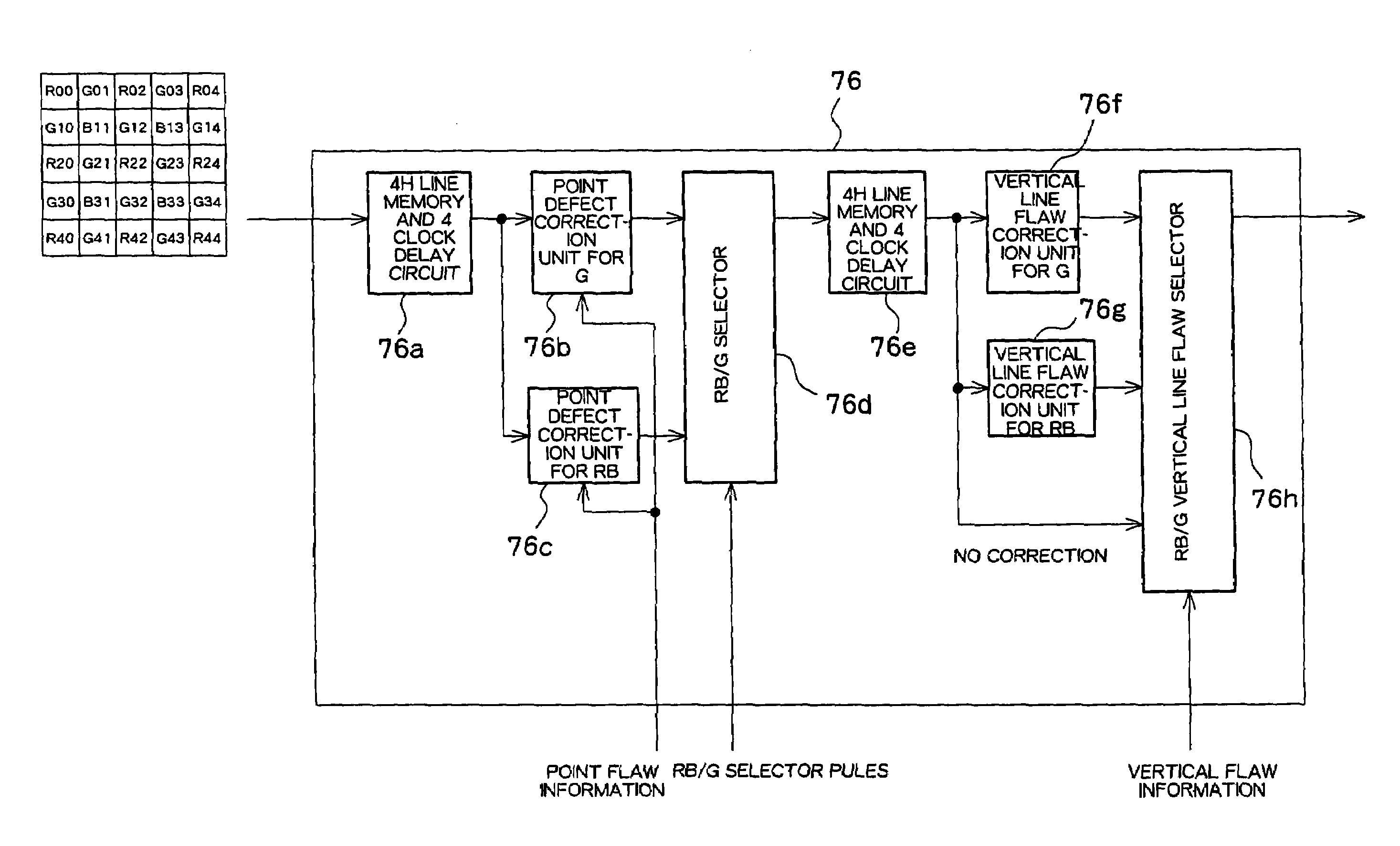
Figure 1 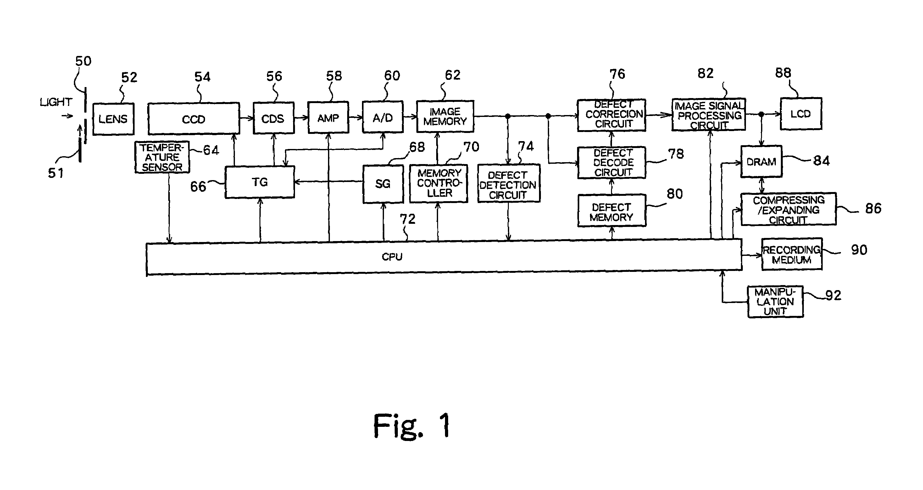
Figure 2 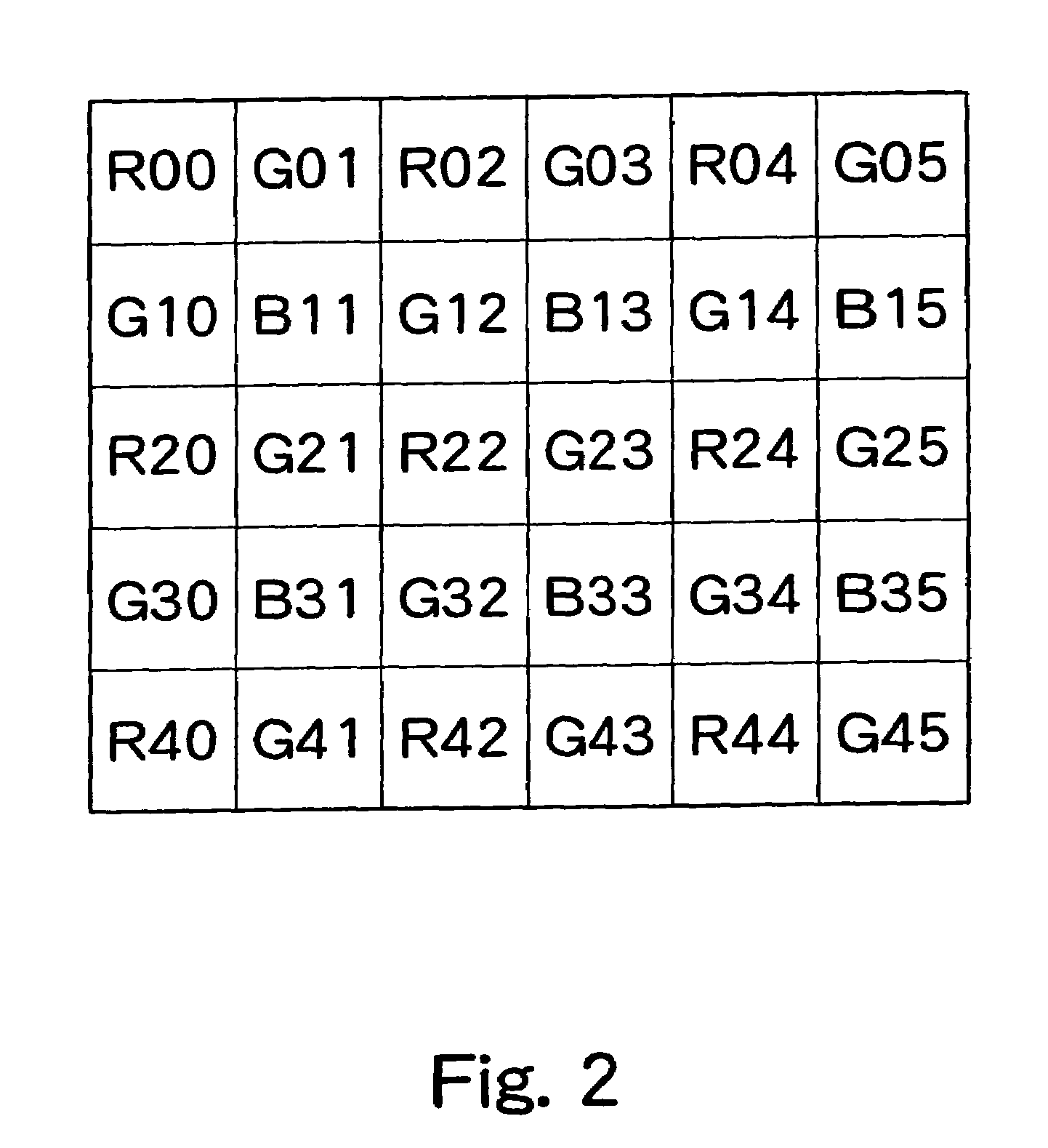
Figure 3
Abstract
Description
FIELD OF THE INVENTION
[0001] The present invention relates to a pixel defect correction device, and in particular to a technique for correcting point defects, horizontal direction defects, and vertical direction defects in two-dimensional pixels arranged along horizontal and vertical directions.BACKGROUND OF THE INVENTION
[0002] CCD's and CMOS's are used as imaging elements in digital cameras. In order to respond to a demand for higher image quality, efforts have been made to reduce pixel size and increase the number of pixels. While the reduction of the pixel size can be achieved by reducing the size of the photodiode and vertical direction (V) transfer path, reduction of the size of the photodiode and the V transfer path increases the probability of generation of defects. A localized crystal defect of a photodiode causes pixel degradation and defects in which a constant bias voltage is always applied to an opto-electric conversion output corresponding to an amount of incident light c...
Examples
Embodiment Construction
[0104]Preferred embodiments of the present invention will now be described referring to the drawings. FIG. 1 shows an overall structure of a digital camera incorporating a pixel defect correction circuit according to a first preferred embodiment of the present invention. An optical system including a diaphragm 50 and a lens 52 guides light from an imaging target to a CCD 54. A light shielding filter 51 may be placed in front of the diaphragm 50. The CCD 54 converts the light from the imaging target into an electrical signal corresponding to the amount of light and supplies the electrical signal to a CDS (correlated double sampling) 56. The CDS 56 samples the image signal and supplied to an A / D 60 through an amplifier (AMP) 58. The amplifier (AMP) 58 adjusts a gain of the image signal. The A / D 60 converts the sampled image signal into a digital signal and supplies the digital signal to an image memory 62 which functions as a frame memory. Operations of the CCD 54, CDS 56, and A / D 60 ...