
Work bonding and supporting method and work bonding and supporting apparatus using the same
a technology of work bonding and supporting apparatus, applied in the direction of chemistry apparatus and processes, other domestic articles, layered products, etc., can solve the problems of elongation of adhesive tape for supporting, more susceptible to adverse influence of wafers with adhesive layers, and the conventional method
Patent Information
- Authority / Receiving Office
- US · United States
- Patent Type
- Patents(United States)
- Current Assignee / Owner
- Publication Date
- 2012-02-07
- Estimated Expiration
- Not applicable · inactive patent
Smart Images
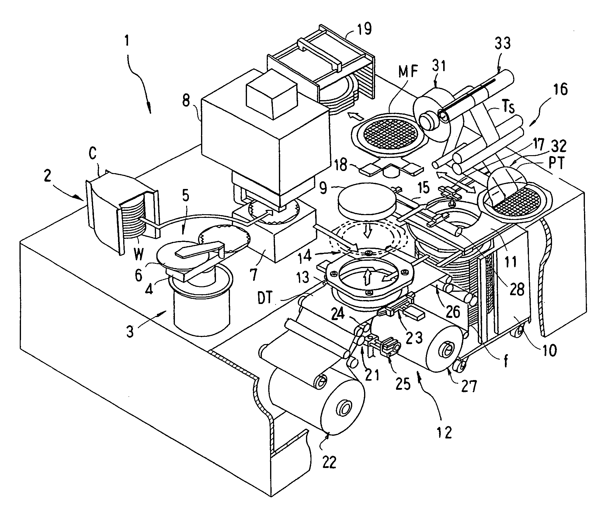
Figure 1 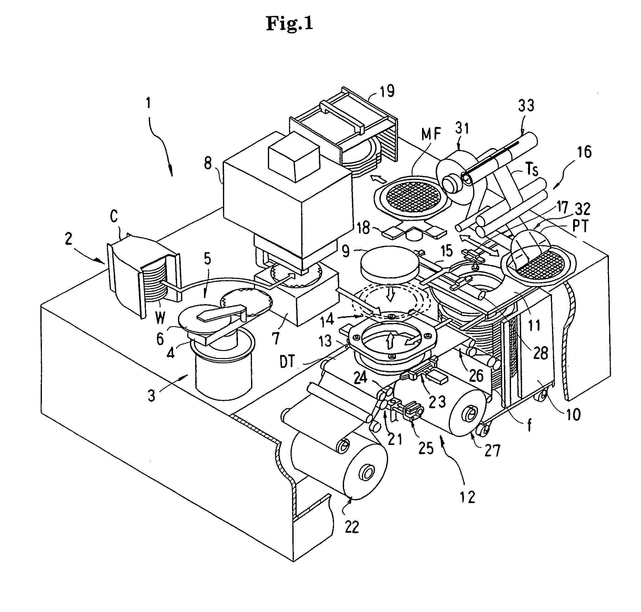
Figure 2 
Figure 3
Abstract
Description
BACKGROUND OF THE INVENTION
[0001] 1. Field of the Invention
[0002] The present invention relates to a method for bonding a work to an adhesive tape for support to support the work as a process performed before carriage of a thin-plate-shaped work such as a semiconductor wafer or a glass substrate and various processes to be performed on the work, and to a work bonding and supporting apparatus using the method.
[0003] 2. Description of the Related Art
[0004] In a process of cutting out semiconductor chips from a semiconductor wafer (hereinbelow, simply called “wafer”) as a representative thin-plate-shaped work, a wafer is supported by being bonded to an adhesive tape for support which is bonded to a ring frame. After that, a dicing process and a chip cutting process are performed on the bonded and supported wafer (refer to Japanese Patent Laid-Open No. 2005-033119).
[0005] The conventional method, however, has the following problems.
[0006] In the process of adhering a wafer to an adhesive tape...
Examples
Embodiment Construction
[0043]Embodiments of a semiconductor wafer mounter utilizing the present invention will be described below with reference to the drawings.
[0044]FIG. 1 is a cutaway perspective view showing a general configuration of a semiconductor wafer mounter including a work bonding and supporting apparatus of the present invention.
[0045]A semiconductor wafer mounter 1 includes a wafer supplying unit 2 in which a cassette C housing wafers (works) W subjected to back grinding process in multiple stages is loaded, a wafer transport mechanism 3 having a robot arm 4 and a pressing mechanism 5, an alignment stage 7 for aligning a wafer W, an ultraviolet irradiating unit 8 for irradiating the wafer W mounted on the alignment stage 7 with ultraviolet rays, a vacuum table 9 holding the wafer W on its under face by vacuum, a ring frame supplying unit 10 housing ring frames “f” in multiple stages, a ring frame transport mechanism 11 for transferring the ring frame “f” onto an adhesive tape DT for support ...