
Power-aware RAM processing
a ram processing and power-aware technology, applied in computing, digital storage, instruments, etc., can solve the problems of time-consuming optimization process, high power consumption of ram processing, and high cost of manual optimization process, so as to reduce power consumption and suppress clock transitions
Patent Information
- Authority / Receiving Office
- US · United States
- Patent Type
- Patents(United States)
- Current Assignee / Owner
- Publication Date
- 2016-05-03
Smart Images
Figure 1 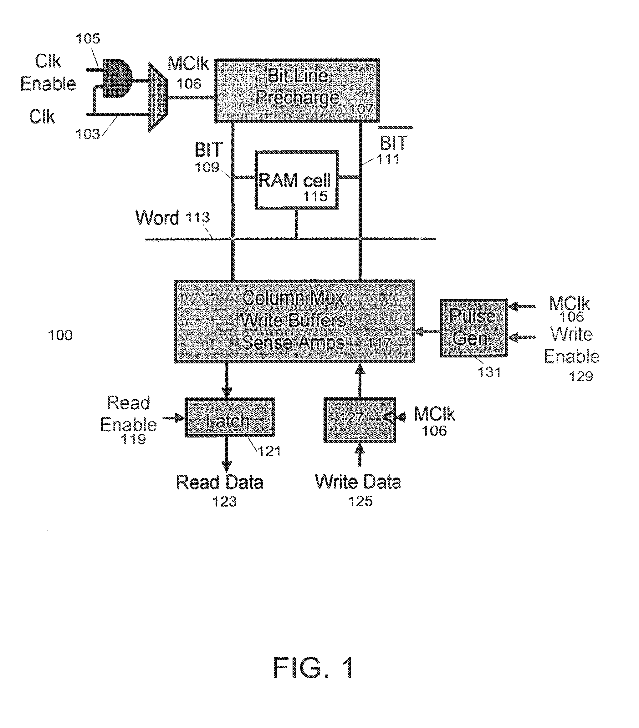
Figure 2 
Figure 3
Abstract
Description
CROSS-REFERENCES TO RELATED APPLICATIONS
[0001] This application is a continuation of, and claims the benefit of and priority to, U.S. patent application Ser. No. 11 / 510,018, filed Aug. 24, 2006 (currently pending), which claims the benefit of and priority to U.S. Provisional Patent Application No. 60 / 719,251, filed Sep. 20, 2005, each of which is incorporated herein by reference in its respective entirety.BACKGROUND OF THE INVENTION
[0002] The present invention relates to the field of programmable devices, and the systems and methods for programming the same. Programmable devices, such as FPGAs, typically includes thousands of programmable logic cells that use combinations of logic gates and / or look-up tables to perform a logic operation. Programmable devices also include a number of functional blocks having specialized logic devices adapted to specific logic operations, such as adders, multiply and accumulate circuits, phase-locked loops, and one or more embedded memory array blocks. ...
Examples
Embodiment Construction
[0026]FIG. 1 illustrates an example embedded memory 100 of a programmable device suitable for use with the optimization techniques of embodiments of the invention. FIG. 1 illustrates a single access port for reading and writing data to embedded memory 100. Other implementations of embedded memory 100 can have multiple access ports, similar to that shown in FIG. 1, enabling read and / or write access to the embedded memory 100.
[0027]Embedded memory 100 receives a clock signal via a clock signal input 103 from another portion of the programmable device. As discussed in detail below, the operation of the programmable device is directed by control signals and the clock signal. In this implementation, the clock signal input 103 is gated with a clock enable signal provided via a clock enable input 105 to produce a memory clock signal 106. The clock enable signal input 103 can be used to selectively deactivate the memory clock signal 106, thereby deactivating the entire embedded memory block...