Plasma display apparatus, driving method thereof and driving IC

A plasma display and display unit technology, applied in identification devices, static indicators, instruments, etc., can solve the problems of damaged phosphors, brightness degradation, uneven brightness, etc., prevent misdischarge and discharge failure, reduce power consumption, brightness Effect of deterioration reduction

Inactive Publication Date: 2009-07-01
HITACHI LTD
View PDF1 Cites 0 Cited by
  • Summary
  • Abstract
  • Description
  • Claims
  • Application Information

AI Technical Summary

Problems solved by technology

[0008] However, the present inventors have found that there are disadvantages such as the following, that is, when the order is Figure 12 In such a drive circuit, the electric power flowing from the Y electrode into the A electrode during the clamping period is large, the potential of the power supply Va rises, etc., making it unstable, and the wall charge formation based on Va during the address period is different for each display cell, so uneven brightness
In addition, the present inventors also found the problem that not only weak discharge between Y electrode and X electrode but also discharge between Y electrode and A electrode occurs during reset, and positive blunt wave reset cannot be smoothly performed. conduct
In addition, it is also known that there is a problem that discharge between the Y electrode and the A electrode also occurs during the reset period and the holding period other than the address period, thereby damaging the phosphor formed on the A electrode side and contributing to deterioration of luminance.

Method used


Image

  • Plasma display apparatus, driving method thereof and driving IC
  • Plasma display apparatus, driving method thereof and driving IC
  • Plasma display apparatus, driving method thereof and driving IC

Examples


Embodiment Construction

[0081] Hereinafter, embodiments of the present invention will be described in detail using the drawings.

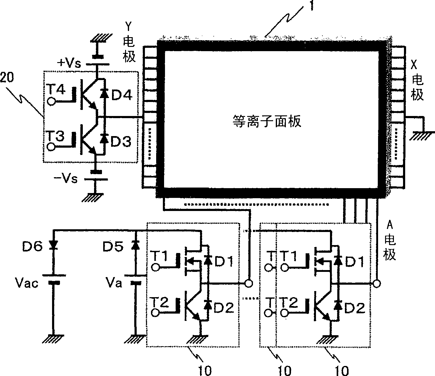
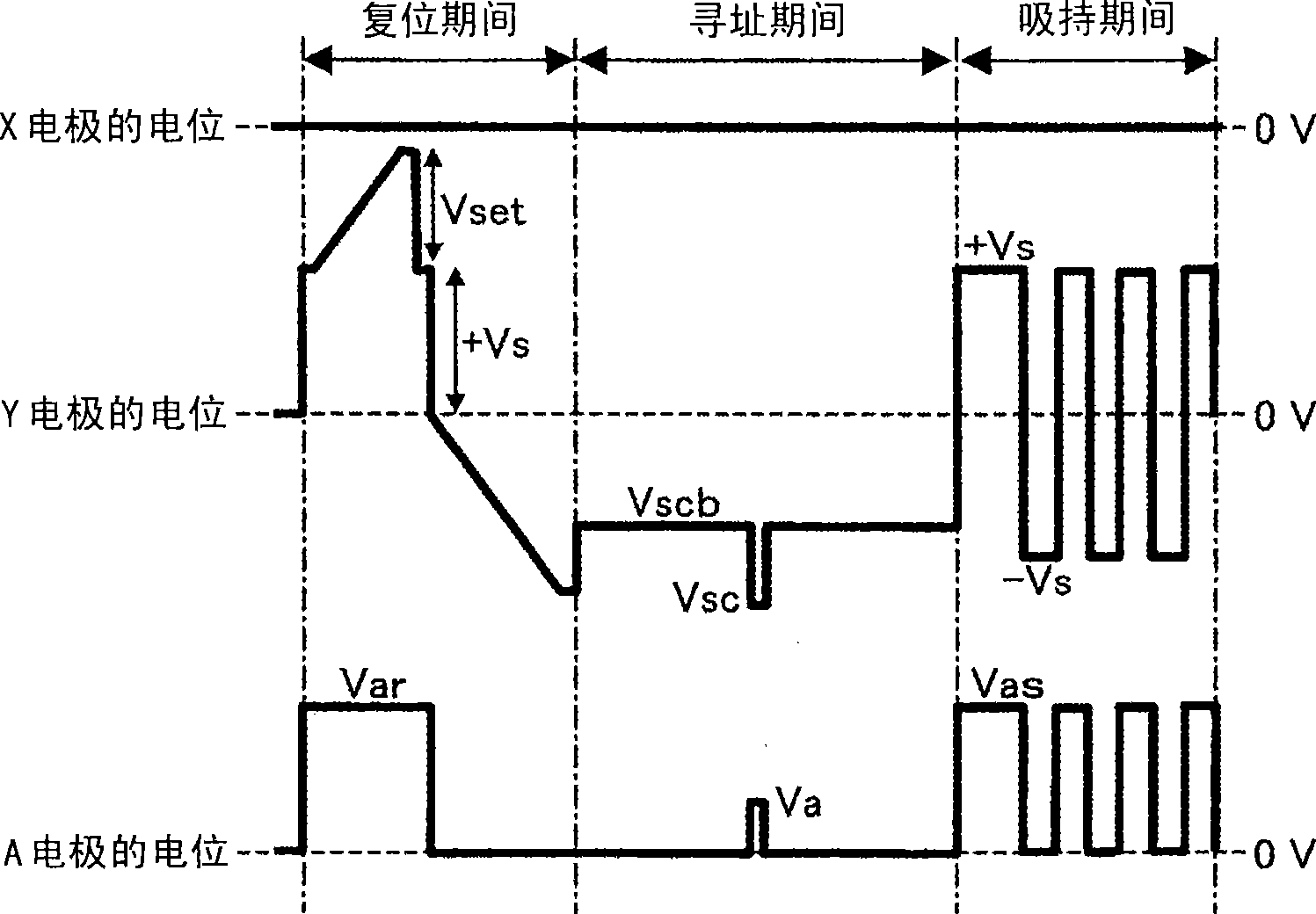
[0082] figure 1 An example of an AC-type PDP device to which the present invention is applied is shown. The X electrodes of the plasma panel are fixed to the ground. The drive circuit 20 is arranged on the Y electrode of the plasma panel, and +Vs and -Vs are alternately applied to the Y electrode by turning T3 and T4 of the IGBT alternately on and off during the clamping period. use figure 2 The driving radio wave of the present invention of the address electrode driving circuit 10 connected to the A electrode will be described in detail.

[0083] During the reset period, not only +Vs for positive blunt wave reset but also Vset is gradually applied to the Y electrode. At this time, the transistors T1 and T2 of the address electrode drive circuit 10 are simultaneously turned off. As the potential of the Y electrode increases, the potential Var of the A electrode ris...


PUM


Abstract

The invention provides a plasma panel display device, a driving method thereof and a driving IC, which can realize the functions that cannot be realized by the current AC typed PDP device of a unilaterally driven holding circuit, such as, stabilizing power supply Va during holding period, inhibiting the discharge of a Y electrode and an A electrode during the reset period, normally realizing blunt wave rest between the Y electrode and the A electrode and effectively utilizing the power of inflow address power. In the course of maintaining the lighting of the AC typed PDP, by fixing the electrode on one side of a panel in a certain potential, and alternatively applying negative and positive voltage to the electrode on the other side of the panel, the device can convert the power of the inflow address power supply into other power supply and ensures the AC typed PDP to have uniform brightness, low consumption and long service life.

Description

technical field [0001] The present invention relates to a PDP (Plasma Display) device, a driving method thereof, and a driving IC. Background technique [0002] In recent years, AC-type plasma display devices have been rapidly popularized because they are larger and thinner than conventional CRT TVs. However, large screens have the problems of high power consumption and high cost. [0003] In the display panel of an AC plasma display, X electrodes and Y electrodes are arranged approximately parallel and alternately, and address electrodes (hereinafter referred to as A electrodes) intersect in a vertical direction with respect to the X electrodes and Y electrodes, forming a two-dimensional matrix. [0004] Figure 11 A conventional example of a plasma panel 1 (also referred to as a display panel) of an AC type PDP device and its main drive circuit is shown. In this circuit, the suction circuit is only located on the Y electrode side, and the potential of the X electrode is f...

Claims


Application Information

Patent Timeline
Patent Type & Authority Applications(China)
IPC IPC(8): G09G3/288G09F9/313G09G3/20G09G3/291G09G3/292G09G3/293G09G3/294G09G3/296G09G3/298H04N5/66
CPCG09G3/294G09G2330/021G09G3/296G09G2330/028G09G2320/0233G09G3/288H01J11/22
Inventor 森睦宏长濑拓生
Owner HITACHI LTD
Why Eureka
Try Eureka