Active matrix substrate, liquid crystal panel, liquid crystal display apparatus, television receiver, and a method for manufacturing active matrix substrate

An active matrix and substrate technology, applied in the field of active matrix substrates, can solve the problems of low ratio of active matrix substrate 905, reduction of ratio of active matrix substrate 905, small range of data signal lines 915, etc.

Inactive Publication Date: 2010-11-10
SHARP KK
View PDF1 Cites 1 Cited by
  • Summary
  • Abstract
  • Description
  • Claims
  • Application Information

AI Technical Summary

Problems solved by technology

[0024] However, the above-mentioned conventional active matrix substrate 905 has the problem that the range in which defective data signal lines 915 can be corrected is small.
In other words, there is a problem that the range of data signal lines 915 that cannot be corrected for defects is wide, and the ratio of active matrix substrates 905 that can remedy broken lines is low.
As a result, the ratio of salvageable defective (disconnected) active matrix substrates 905 is reduced

Method used


Image

  • Active matrix substrate, liquid crystal panel, liquid crystal display apparatus, television receiver, and a method for manufacturing active matrix substrate
  • Active matrix substrate, liquid crystal panel, liquid crystal display apparatus, television receiver, and a method for manufacturing active matrix substrate
  • Active matrix substrate, liquid crystal panel, liquid crystal display apparatus, television receiver, and a method for manufacturing active matrix substrate

Examples


Embodiment Construction

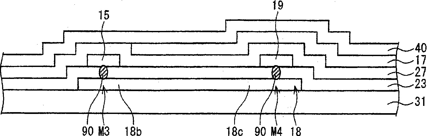
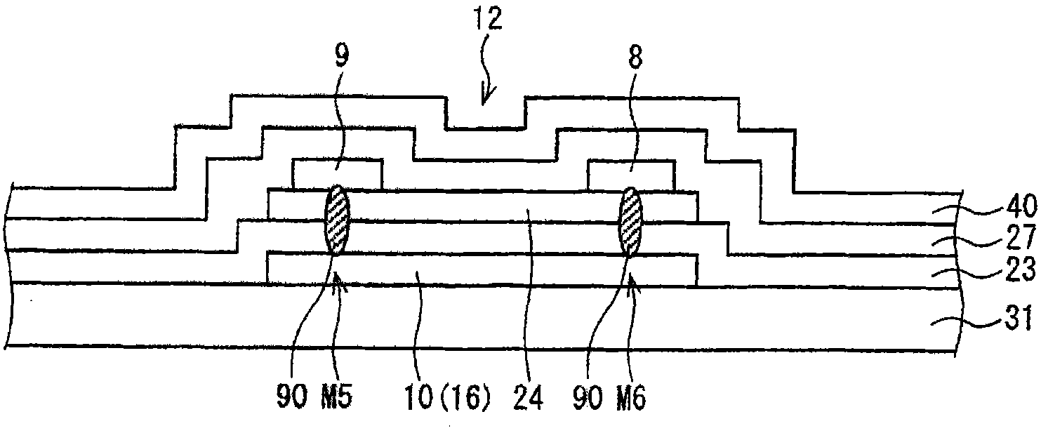
[0103] Next, various embodiments of the present invention will be described. In addition, in each structure (each figure), the same code|symbol is attached|subjected to the member with a common function, and description is abbreviate|omitted as appropriate.

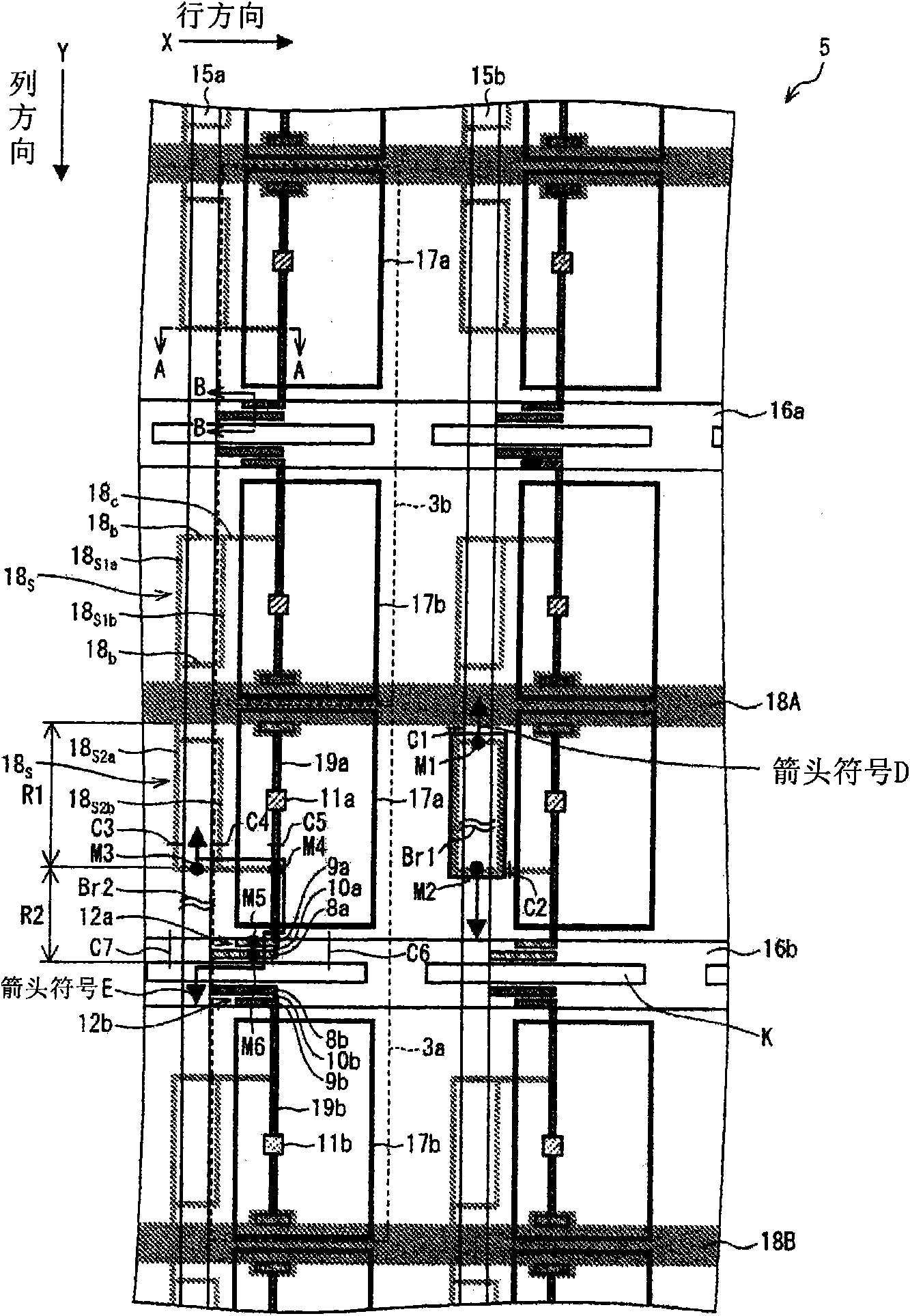
[0104] figure 1 The structure of the active matrix substrate 5 of this embodiment is shown.

[0105] (data signal line, scan signal line, holding capacitor wiring)

[0106] In the present active matrix substrate 5 of the pixel division method, as described above figure 1 As shown, there are provided: data signal lines 15 (15a·15b) extending along the column direction Y, scanning signal lines 16 (16a·16b) extending along the row direction X, and storage capacitor wirings 18 extending along the row direction X ( 18A·18B), the pixel regions 3 are arranged in a matrix, and the data signal lines 15 intersect with the storage capacitor lines 18 and the scanning signal lines 16 through an insulating layer (not shown).

[0...


PUM


Abstract

The invention provides an active matrix substrate, a liquid crystal panel, a liquid crystal display apparatus, a television receiver, and a method for manufacturing the active matrix substrate. The active matrix substrate comprising retention volume wiring extended portions (18s) each extending from an intersection between a retention volume wiring (18A) and a data signal line (15a) toward two intersections between two scanning signal lines (16a, 16b) adjacent to each other and the data signal line (15a). The retention volume wiring extended portions (18s) each includes an overlapping portion (M3) which overlaps with the data signal line (15a), and a retention volume wiring secondary extended portion (18c), which is further extended from the retention volume wiring extended portions (18s), includes an overlapping portion (M4) which overlaps with a drain lead-out wire (19a), and at least one side of an opening (K) of the scanning signal line (16b) functions as a gate electrode (10a) of a transistor (12a).

Description

technical field [0001] The present invention relates to an active matrix substrate capable of correcting a disconnection of a data signal line, a liquid crystal panel using the active matrix substrate, and the like. Background technique [0002] Figure 5 A conventional structure of an active matrix substrate 905 having a multi-pixel structure (pixel division method) is shown. [0003] As shown in the figure, the active matrix substrate 905 includes data signal lines 915 extending in the column direction Y, scanning signal lines 916 extending in the row direction X, storage capacitor wiring 918 extending in the row direction X, and The pixel area 903 divided by the data signal line 915 and the above-mentioned scanning signal line 916 . [0004] The storage capacitor wiring 918 crosses the center of the pixel region 903 , and the transistor 912 and the pixel electrode 917 are formed in the pixel region 903 . [0005] Specifically, in the pixel region 903 , the source electr...

Claims


Application Information

Patent Timeline
Patent Type & Authority Applications(China)
IPC IPC(8): G02F1/1368G09F9/00G09F9/30
CPCG02F1/136204G02F1/136286G02F1/136213
Inventor 山下祐树
Owner SHARP KK
Why Eureka
Try Eureka