Method for realizing high-download rate photonic crystal demultiplexer with reflection micro-cavity employing implantation technology

A demultiplexer and photonic crystal technology, which is applied in the field of optical communication, can solve the problems of low download efficiency of the demultiplexer, high manufacturing precision of the photonic crystal air hole structure resonant cavity, and signal interference.

CN102269844BInactive Publication Date: 2014-04-02BEIJING UNIV OF POSTS & TELECOMM
3 Cites 2 Cited by

Patent Information

Authority / Receiving Office
CN · China
Patent Type
Patents(China)
Current Assignee / Owner
Publication Date
2014-04-02
Estimated Expiration
Not applicable · inactive patent

Smart Images

  • Figure 1
    Figure 1
  • Figure 2
    Figure 2
  • Figure 3
    Figure 3
Patent Text Reader

Abstract

The invention relates to a method for realizing a high-download rate photonic crystal demultiplexer with a reflection micro-cavity employing an implantation technology. In the method, a device structure for introducing the reflection micro-cavity and a microfluid implantation technology into a two-dimensional photonic crystal demultiplexer is designed, and a higher download rate is acquired by increasing the reflection micro-cavity at a specific position on the rear side of a download micro-cavity along a main waveguide direction; and microfluid with different refractive indexes is implanted into an air hole of a resonant cavity at different positions of the demultiplexer, so that a guide die of a photonic crystal is changed, a transmission peak shifts, and multi-channel wavelength demultiplexing is realized. The photonic crystal having a medium background air hole structure in a triangular lattice is utilized, and the method is closer to a silicon-on-insulator (SOI)-based photonic crystal manufacturing technology which is widely applied at present, and is high in realizability. The three channels have the transmissivity of over 95 percent, and good application of the method in photon integration and wavelength division multiplexing (WDM) can be acquired.
Need to check novelty before this filing date? Find Prior Art

Description

Technical field

[0001] The invention relates to a method for realizing a high download rate photonic crystal demultiplexer using injection technology and a reflective microcavity, and belongs to the technical field of optical communication. Background technique

[0002] With the large-scale application of wavelength division multiplexing (WDM) technology in communication systems, many demultiplexers of different structures have been proposed and extensively studied. So far, demultiplexers mainly include semiconductor demultiplexers (Document 1, Koichi Takiguchi, Tsutomu Kitoh, Manabu Oguma, Atsushi Mori, and Hiroshi Takahashi, "Integrated-optic demultiplexers for optical OFDM signals," Optical Fiber Communication Conference (OFC) 2011, and Literature 2, Jianjun Chen, Zhi Li, Jia Li, and Qihuang Gong, "Compact and high-resolution plasmonic wavelength demultiplexers based on Fano interference," Optics Express, Vol.19 Issue 10, pp.9976- 9985 (2011)), metal grating demultiplexer (Do...

Examples

Embodiment Construction

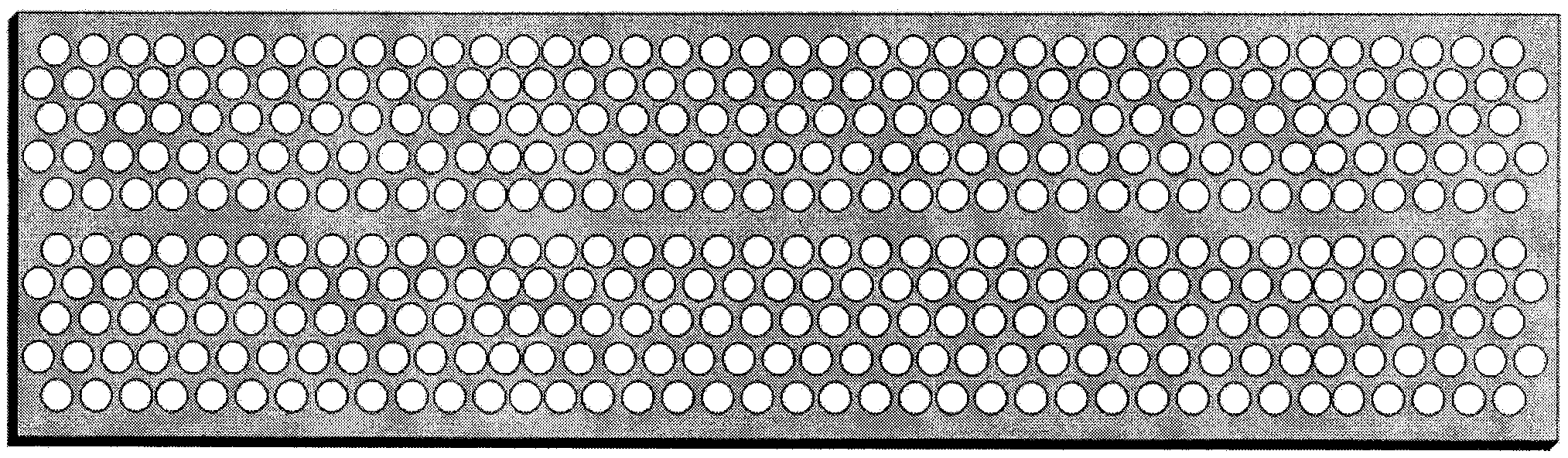
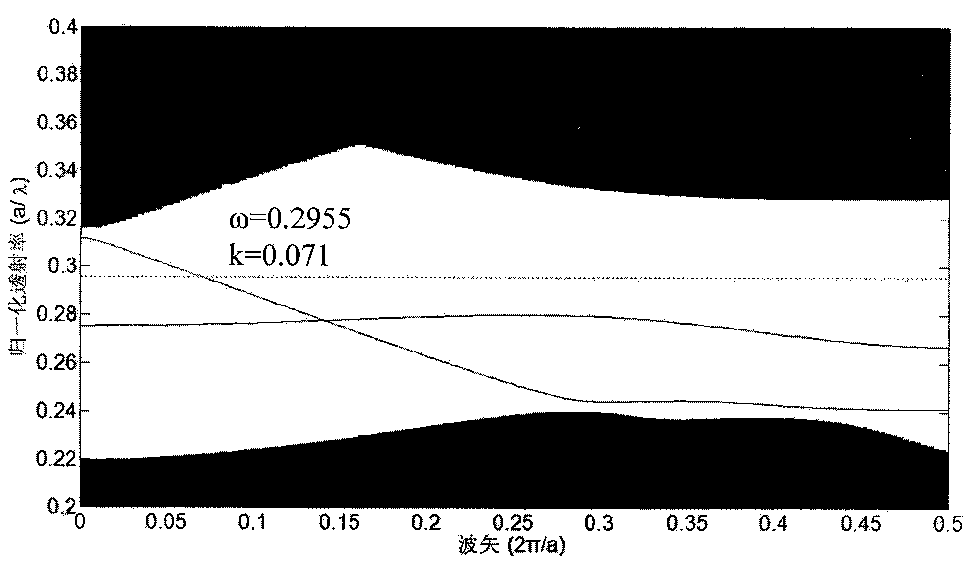
[0036] The structure of the photonic crystal demultiplexer with reflective microcavity using injection technology is as follows figure 1 As shown, it contains the W1 photonic crystal waveguide and three pairs of download and coupling microcavities. The download cavity is the second row of the W1 waveguide. One air hole is removed. It is composed of six air holes adjacent to the air hole. The radius of the air hole near the W1 waveguide and the drop waveguide is 0.23a, and the radius of the remaining air holes is still 0.4. a. Lattice constant a=445nm, ordinary air hole radius r=182nm, refractive index of dielectric silicon n si = 3.48. Since the refractive index of the air hole will affect the change of the resonant frequency, the basic structure of the photonic crystal multi-channel demultiplexer can be formed by reasonable design of the refractive index of the injected microfluid.

[0037] First, determine the distance between the coupling cavities through the band diagram of...