Encapsulation structure of fingerprint recognition sensor, electronic device and preparation method of fingerprint recognition sensor

A fingerprint recognition and packaging structure technology, applied in character and pattern recognition, instruments, computer parts, etc., can solve the problems of thick electronic equipment, high cost, and expensive production of fingerprint recognition sensors.

Active Publication Date: 2017-06-06
NANCHANG OUFEI BIOLOGICAL IDENTIFICATION TECH
View PDF3 Cites 0 Cited by
  • Summary
  • Abstract
  • Description
  • Claims
  • Application Information

AI Technical Summary

Problems solved by technology

[0002] The traditional fingerprint recognition sensor forms a matrix fingerprint recognition sensor through the CMOS semiconductor process. Since the fingerprint imaging sensor with the silicon substrate as the substrate is easy to be brittle, a protective lens with high hardness and scratch resistance (such as sapphire) is required. The cost of sapphire is High lead to expensive production of capacitive fingerprint recognition sensors based on monocrystalline silicon
At the same time, the fingerprint recognition sensor is prepared to be embedded in the shell of the electronic device in a packaging structure, and the use of sapphire will also lead to a larger thickness of the fingerprint recognition sensor package and the electronic device

Method used


Image

  • Encapsulation structure of fingerprint recognition sensor, electronic device and preparation method of fingerprint recognition sensor
  • Encapsulation structure of fingerprint recognition sensor, electronic device and preparation method of fingerprint recognition sensor
  • Encapsulation structure of fingerprint recognition sensor, electronic device and preparation method of fingerprint recognition sensor

Examples


Embodiment Construction

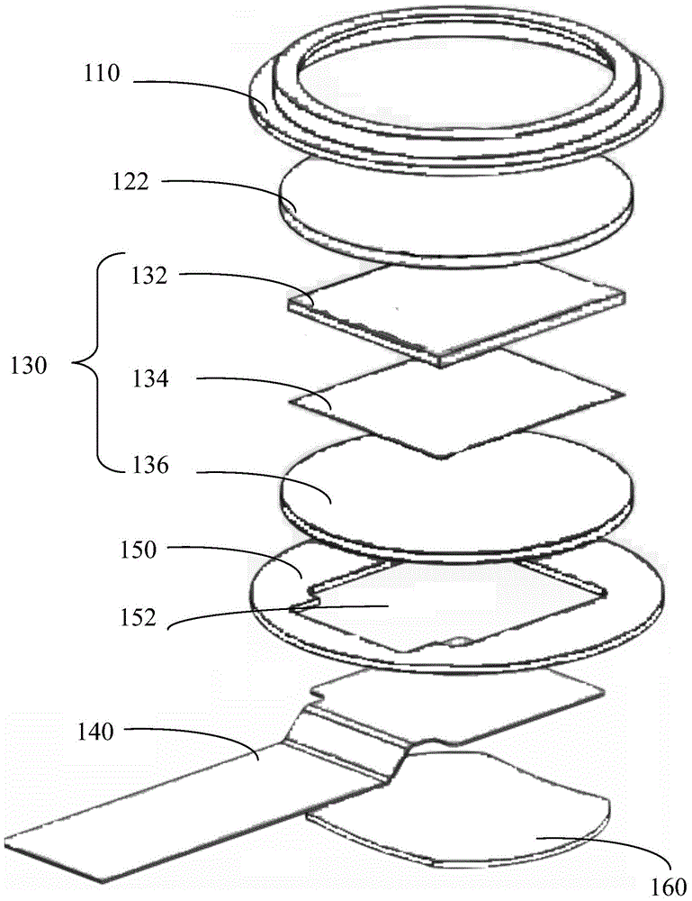
[0026] Please refer to figure 1 , illustrating an exploded state of a package structure of a fingerprint recognition sensor used in an electronic device. The electronic device here should be understood in a broad sense, and can be a smart phone, a touch panel, a mobile computing device, an electrical appliance, a panel or body of a vehicle, and the like.

[0027] The packaging structure of the fingerprint recognition sensor includes a base ring 110 made of metal material, a control button surrounded by the base ring 110, a fingerprint recognition sensor 130 placed under the control button, a flexible element 140 and a strengthening element 150 placed under the fingerprint recognition sensor 130 , and a dome switch 160 placed under the reinforcing element 150 .

[0028] The control button is configured above and coupled to the circuit of the fingerprint identification sensor 130 . In an electronic device, a control button may be arranged relative to a display element of the e...


PUM


Abstract

The invention relates to a fingerprint recognition sensor packaging structure and an electronic device with the fingerprint recognition sensor packaging structure. The fingerprint recognition sensor packaging structure comprises a control button and a fingerprint recognition sensor arranged below the control button, wherein the control button comprises a glass cover plate and a thin film which coats the surface of the glass cove plate and is made of non-anisotropic dielectric materials. The mode of combining the glass cover plate and the coated film is adopted by the control button, the hardness of the control button is ensured, meanwhile, cost is reduced, in addition, the thickness of the fingerprint recognition sensor packaging structure is not affected, and when the fingerprint recognition sensor packaging structure is embedded into the electronic device, the thickness design of the electronic device is not affected.

Description

technical field [0001] The invention relates to the field of electronic sensing, in particular to a fingerprint identification sensor packaging structure, electronic equipment using the fingerprint identification packaging structure, and a preparation method of the fingerprint identification sensor. Background technique [0002] The traditional fingerprint recognition sensor forms a matrix fingerprint recognition sensor through the CMOS semiconductor process. Since the fingerprint imaging sensor with the silicon substrate as the substrate is easy to be brittle, a protective lens with high hardness and scratch resistance (such as sapphire) is required. The cost of sapphire is High makes monocrystalline silicon-based capacitive fingerprint recognition sensors expensive to produce. At the same time, the fingerprint identification sensor is prepared to be embedded in the shell of the electronic device in a packaging structure, and the use of sapphire will also result in a larger...

Claims


Application Information

Patent Timeline
Patent Type & AuthorityPatents(China)
IPC IPC(8): G06K9/00
Inventor刘隆主杜东阳白安鵬蔡美雄
OwnerNANCHANG OUFEI BIOLOGICAL IDENTIFICATION TECH