Display substrate, display panel and display device

A technology for display substrates and display panels, applied in optics, instruments, electrical digital data processing, etc., can solve problems such as high power consumption, and achieve the effect of reducing power consumption

Active Publication Date: 2015-03-11
XIAMEN TIANMA MICRO ELECTRONICS +1
View PDF6 Cites 21 Cited by
  • Summary
  • Abstract
  • Description
  • Claims
  • Application Information

AI Technical Summary

Problems solved by technology

[0006] In view of this, an embodiment of the present invention provides a display substrate, a display panel, and a display device to solve the technical problem of high power consumption of a touch display device using a capacitive touch panel in the prior art

Method used


Image

  • Display substrate, display panel and display device
  • Display substrate, display panel and display device
  • Display substrate, display panel and display device

Examples


Embodiment Construction

[0036] The present invention will be further described in detail below in conjunction with the accompanying drawings and embodiments. It should be understood that the specific embodiments described here are only used to explain the present invention, but not to limit the present invention. In addition, it should be noted that, for the convenience of description, only parts related to the present invention are shown in the drawings but not all content.

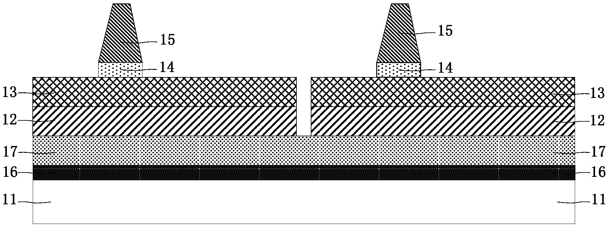
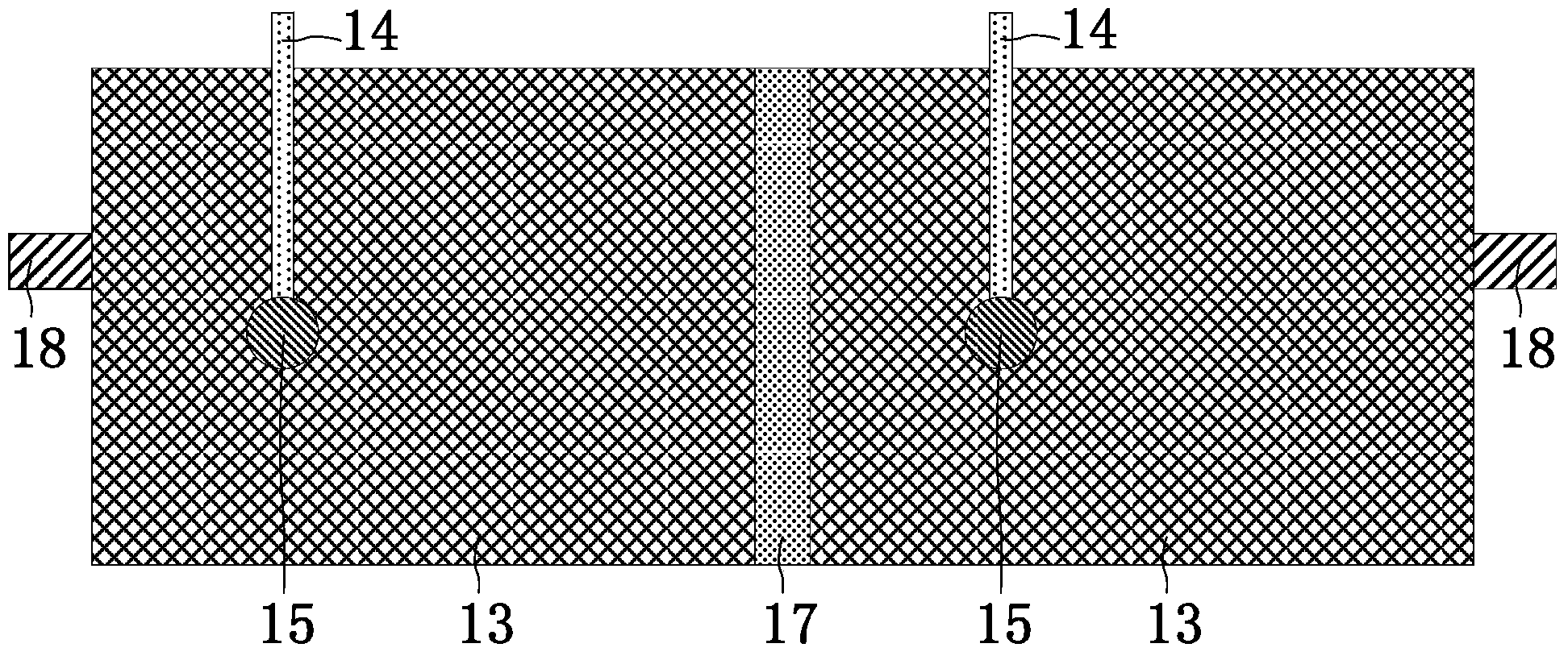
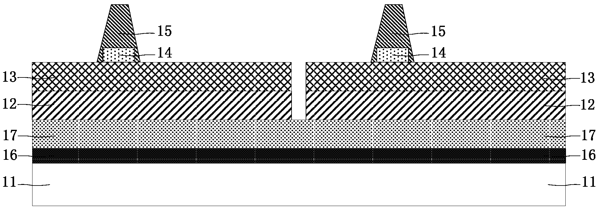
[0037] An embodiment of the present invention provides a display substrate. figure 1 It is a schematic structural diagram of a combination of a display substrate and a main column spacer provided by an embodiment of the present invention. Such as figure 1 As shown, the display substrate includes: a substrate 11; at least one conductive layer 12 arranged on the substrate 11; a plurality of patterned piezoelectric layers 13 arranged on the conductive layer 12; arranged on the pattern A plurality of first wires 14 on the piezoe...


PUM

PropertyMeasurementUnit
thicknessaaaaaaaaaa

Abstract

The invention discloses a display substrate, a display panel and a display device. The display substrate comprises a substrate, at least one conducting layer, a plurality of patterned piezoelectric layers, a plurality of first conducting wires and a plurality of main columnar shock insulator bodies, wherein the conducting layer is arranged on the substrate; the plurality of patterned piezoelectric layers are arranged on the conducting layer; the first conducting wires are arranged on the patterned piezoelectric layers; the main columnar shock insulator bodies correspond to the first conducting wires, when the touch occurs, pressure of the main columnar shock insulator bodies on the corresponding patterned piezoelectric layers is converted into electric signals through the patterned piezoelectric layers, and the electric signals are outputted through the first conducting wires. According to the technical scheme, while the touch function of the display panel and the display device is realized, the power consumption is also reduced, so that a power-saving effect can be realized.

Description

technical field [0001] The present invention relates to the field of display technology, in particular to a display substrate, a display panel and a display device. Background technique [0002] With the development of modern electronic technology, the touch technology is applied to the display device to produce a touch display device, and the application of the touch display device is more and more extensive. [0003] The touch display device can be implemented by using the plug-in touch technology and the embedded touch technology. The plug-in touch technology is to add a touch panel outside the display panel, which will greatly increase the weight of the display device. , does not meet the market's requirements for thinner and lighter display devices; embedded touch technology is mainly divided into On-Cell touch technology and In-Cell touch technology, of which On-Cell touch technology is a combination of projected capacitive touch technology The sensing electrode (Sens...

Claims


Application Information

Patent Timeline
Patent Type & Authority Applications(China)
IPC IPC(8): G02F1/1333G02F1/1339G06F3/044
CPCG02F1/13338G02F1/13394G06F3/0414
Inventor 刘晓敏
Owner XIAMEN TIANMA MICRO ELECTRONICS
Why Eureka
Try Eureka