Pixel circuit, organic electroluminescent display panel and display device
What is AI technical title?
AI technical title is built by Patsnap AI team. It summarizes the technical point description of the patent document.
A pixel circuit and light-emitting module technology, applied in optics, nonlinear optics, static indicators, etc., can solve problems such as high production cost, heavy display screen, and complex circuit structure
Active Publication Date: 2015-01-21
HEFEI XINSHENG OPTOELECTRONICS TECH CO LTD +1
View PDF5 Cites 20 Cited by
Summary
Abstract
Description
Claims
Application Information
AI Technical Summary
This helps you quickly interpret patents by identifying the three key elements:
Problems solved by technology
Method used
Benefits of technology
Problems solved by technology
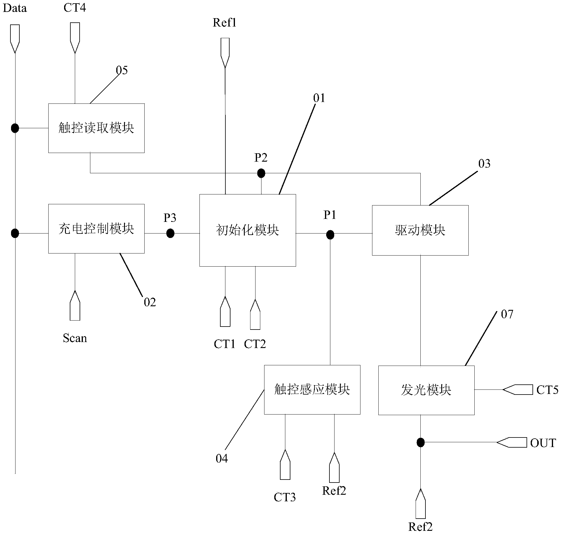
[0004] In the existing built-in touch screen OLED display panel, the circuits generally used to realize the display drive and touch drive are designed separately, that is, one set of circuits is used to realize the touch function, and the other set of circuits is used to realize the OLED display panel. The display driving function, and the display driving circuit and the touch circuit are set separately, there will be disadvantages such as complicated circuit structure, high production cost, heavy and thick display screen
Method used
Image
Click on the blue label to locate the original text in one second.
Reading with bidirectional positioning of images and text.
Examples
Embodiment 1
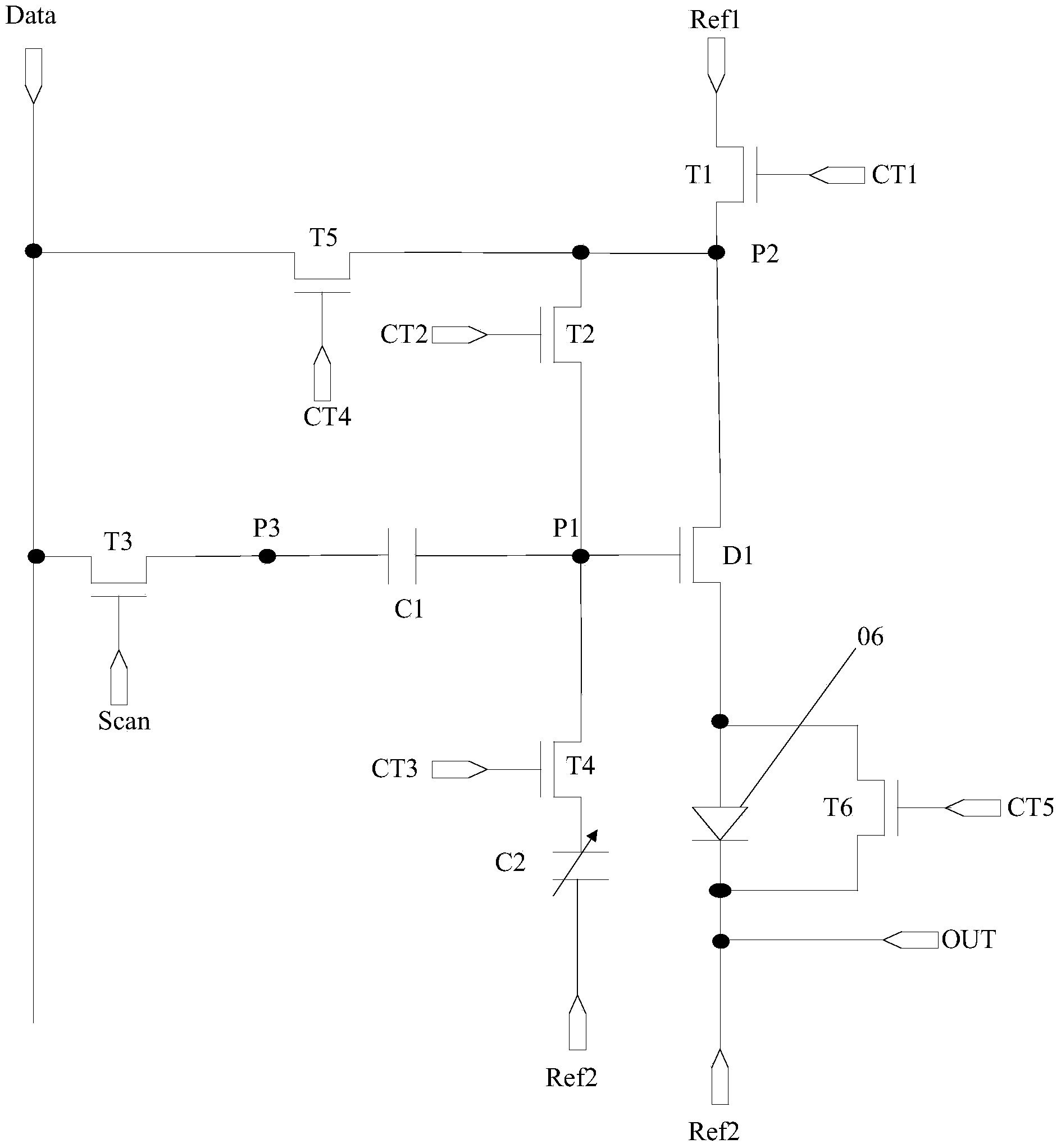
[0057] Example 1: Combining Figure 2a The pixel circuit shown as well as Figure 3a shown Figure 2a The input and output timing diagrams describe the working process of the pixel circuit provided by the embodiment of the present invention. Specifically, choose the Figure 3a There are seven stages of t1-t7 in the input and output sequence diagram shown. In the following description, 1 represents a high-level signal, and 0 represents a low-level signal.
[0058] In the t1 stage, CT1=1, CT2=1, CT3=0, CT4=0, CT5=1, Scan=1, Ref1=Vini, Ref2=0, Data=VL. Because CT1=1, CT2=1, CT5=1, Scan=1, so the first switch transistor T1, the second switch transistor T2, the third switch transistor T3 and the sixth switch transistor T6 conduction; Because CT3=0, CT4 =0, so the fourth switching transistor T4 and the fifth switching transistor T5 are turned off. The turned-on sixth switch transistor T6 conducts the drain of the driving transistor D1 with the second reference signal terminal ...
Embodiment 2
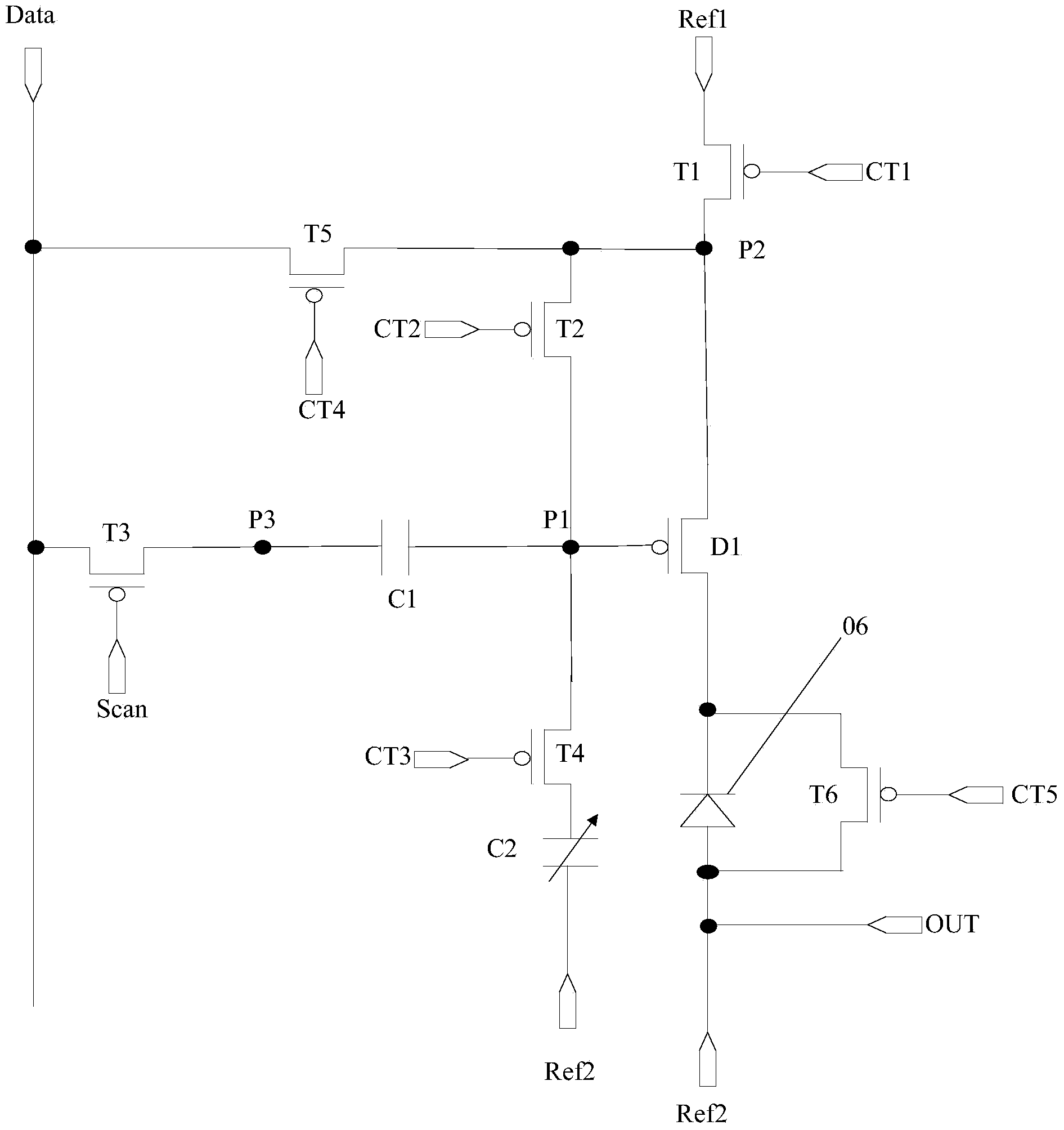
[0066] Embodiment 2: Combination Figure 2c The pixel circuit shown as well as Figure 3b shown Figure 2c The input and output timing diagrams describe the working process of the pixel circuit provided by the embodiment of the present invention. Specifically, choose the Figure 3b There are seven stages of t1-t7 in the input and output sequence diagram shown. In the following description, 1 represents a high-level signal, and 0 represents a low-level signal.
[0067]In the t1 stage, CT1=0, CT2=0, CT3=1, CT4=1, CT5=0, Scan=0, Ref1=Vini, Ref2=1, Data=VL. Because CT1=0, CT2=0, CT5=0, Scan=0, so the first switch transistor T1, the second switch transistor T2, the third switch transistor T3 and the sixth switch transistor T6 conduction; Because CT3=1, CT4 =1, so the fourth switching transistor T4 and the fifth switching transistor T5 are turned off. The turned-on sixth switch transistor T6 conducts the drain of the driving transistor D1 with the second reference signal termi...
PUM
Abstract
The invention discloses a pixel circuit, an organic electroluminescent display panel and a display device. The pixel circuit is characterized in that a first node is initialized in the initializing time periods of a touch control phase and a display phase; the voltage of the first node is regulated in the touch control induction time period; a driving module is enabled to output a corresponding touch control signal under the control of the voltage of the first node in the touch control reading time period for realizing a touch control function; data writing is performed on the first node in the compensation and data writing time period of the display phase; the driving module is enabled to drive a light emitting device in a light emitting module to emit light in a light emitting time period for realizing the normal light emitting function of the light emitting device. Thus, compared with a traditional pixel circuit, the pixel circuit provided by the embodiment of the invention integrates the touch control function and a display function, so that the manufacturing cost of respectively arranging a display driving circuit and a touch control circuit can be reduced; the circuit structure is simplified; and the thickness of the display panel can also be reduced.
Description
technical field [0001] The invention relates to the field of display technology, in particular to a pixel circuit, an organic electroluminescent display panel and a display device. Background technique [0002] With the advancement of display technology, organic light-emitting display (OLED, Organic Light Emitting Diode) is one of the hot spots in the field of flat panel display research today, and more and more active matrix organic light-emitting diodes (AMOLED, Active Matrix Organic Light Emitting Diode) Display panels have entered the market. Compared with traditional thin film transistorliquid crystal display panels (TFT LCD, Thin Film TransistorLiquid Crystal Display), AMOLED has faster response speed, higher contrast ratio and wider viewing angle. [0003] At present, as display devices are developing toward thinner, lighter, higher-resolution, intelligent, and energy-saving devices, touch screen panels (Touch Screen Panels) are more and more widely used. At presen...
Claims
Application Information
Patent Timeline
Application Date:The date an application was filed.
Publication Date:The date a patent or application was officially published.
First Publication Date:The earliest publication date of a patent with the same application number.
Issue Date:Publication date of the patent grant document.
PCT Entry Date:The Entry date of PCT National Phase.
Estimated Expiry Date:The statutory expiry date of a patent right according to the Patent Law, and it is the longest term of protection that the patent right can achieve without the termination of the patent right due to other reasons(Term extension factor has been taken into account ).
Invalid Date:Actual expiry date is based on effective date or publication date of legal transaction data of invalid patent.

