
Semiconductor device and preparation method thereof
A manufacturing method and semiconductor technology, which can be used in the manufacture of semiconductor/solid-state devices, semiconductor devices, electric solid-state devices, etc., and can solve the problems of complex integration process, difficulty in controlling threshold voltage variability, random fluctuation of dopants, etc.
- Summary
- Abstract
- Description
- Claims
- Application Information
AI Technical Summary
Problems solved by technology
Method used
Image

Examples
Embodiment 1
[0100] An embodiment of the present invention provides a method for manufacturing a semiconductor device. The method realizes the adjustment of the threshold voltage of the transistor by adding a cap layer (cap layer) and a barrier layer (barrier layer) in the gate stack structure, which can be more Semiconductor devices with multiple threshold voltages are well realized.
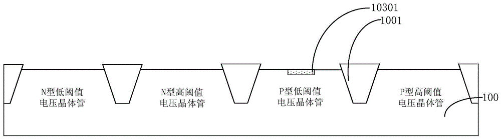
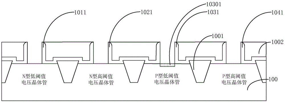
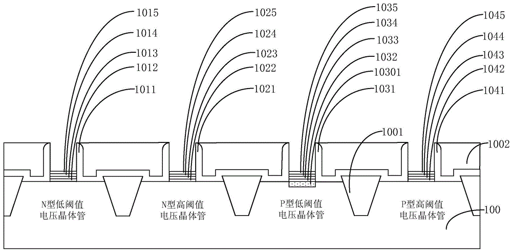
[0101] Below, refer to Figure 1A to Figure 1H as well as Figure 3A A method for manufacturing a semiconductor device proposed in Embodiment 1 of the present invention will be described. in, Figure 1A to Figure 1H A schematic cross-sectional view of a structure formed in the relevant steps of a method for manufacturing a semiconductor device according to an embodiment of the present invention; Figure 3A It is a typical flowchart of a manufacturing method of a semiconductor device according to an embodiment of the present invention.
[0102] The method for manufacturing a semiconductor device according ...
Embodiment 2
[0167] The embodiment of the present invention provides another method for manufacturing a semiconductor device, which also realizes the adjustment of the threshold voltage of the transistor by adding a cap layer (cap layer) and a barrier layer (barrier layer) in the gate stack structure, Semiconductor devices with multiple threshold voltages can be better realized. The difference from Embodiment 1 is that the manufacturing method of the semiconductor device in this embodiment omits the step of forming a silicon germanium layer in the channel region of the P-type low-voltage transistor, and adds the step of forming a fourth function in the P-type low-voltage transistor. Function metal layer steps.
[0168] Below, refer to Figure 2A to Figure 2G as well as Figure 3B A method for manufacturing a semiconductor device proposed in Embodiment 2 of the present invention will be described. in, Figure 2A to Figure 2G A schematic cross-sectional view of a structure formed in the ...
Embodiment 3
[0220] An embodiment of the present invention provides a semiconductor device, which can be manufactured by using the method for manufacturing the semiconductor device in the first embodiment above.
[0221] Below, refer to Figure 4 The structure of a semiconductor device proposed in Embodiment 3 of the present invention will be described. in, Figure 4 It is a schematic cross-sectional view of the structure of a semiconductor device according to an embodiment of the present invention.
[0222] Such as Figure 4 As shown, the semiconductor device of this embodiment includes: a semiconductor substrate 100 and an N-type low-threshold voltage transistor, an N-type high-threshold voltage transistor, a P-type low-threshold voltage transistor, and a P-type high-threshold voltage transistor located on the semiconductor substrate 100 . Wherein, the N-type low-threshold voltage transistor, the N-type high-threshold voltage transistor, the P-type low-threshold voltage transistor, a...
PUM
 Abstract
Description
Claims
Application Information