Manufacturing method for resin plug hole in PCB

A production method and technology of resin plugging holes, which are applied in the direction of printed circuit manufacturing, processing step sequence, electrical components, etc., can solve the problems of shortening the process flow, affecting the production accuracy of the subsequent process, and board expansion and contraction, so as to shorten the production process and ensure The effect of manufacturing precision and simplifying the production process

Active Publication Date: 2015-04-22
JIANGMEN SUNTAK CIRCUIT TECH
View PDF3 Cites 6 Cited by
  • Summary
  • Abstract
  • Description
  • Claims
  • Application Information

AI Technical Summary

Problems solved by technology

[0003] The present invention aims at the problem that the production process of the existing PCB resin plug holes requires abrasive belt grinding to cause expansion and contraction of the board, thereby affecting the producti...

Method used


Image

  • Manufacturing method for resin plug hole in PCB
  • Manufacturing method for resin plug hole in PCB
  • Manufacturing method for resin plug hole in PCB

Examples


Embodiment

[0019] This embodiment provides a method for manufacturing a resin plug hole in a PCB. The parameters of the PCB manufactured by this method are as follows:

[0020]

[0021] The specific production steps are as follows:

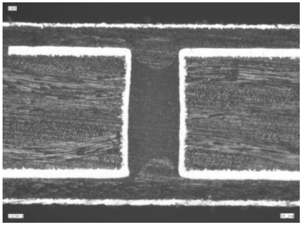
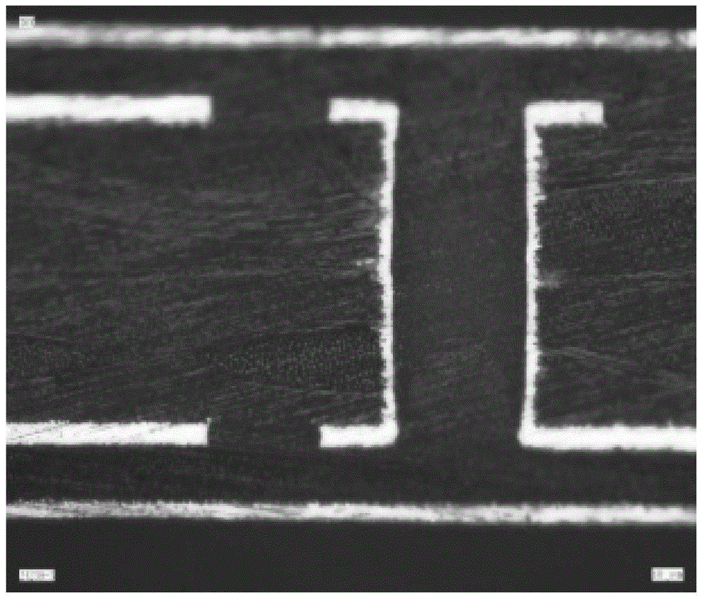
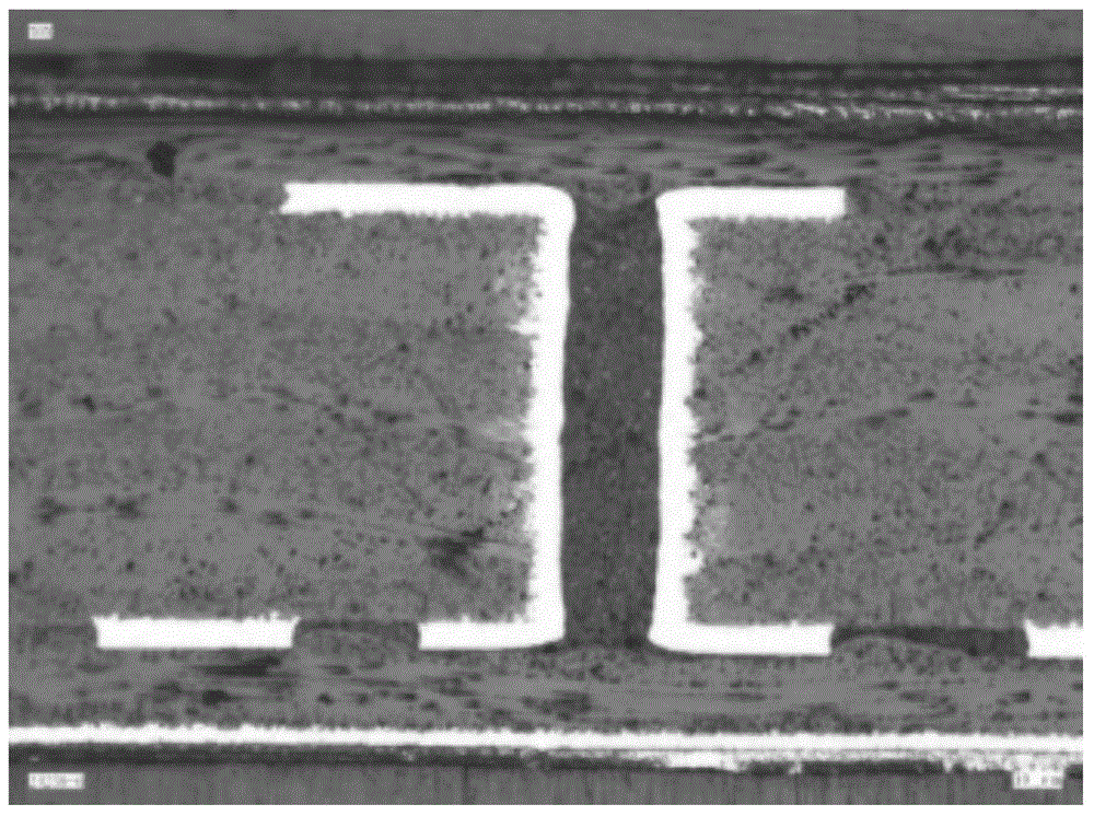
[0022] (1) First cut the base material, the thickness of the core board is 1.2mm H / H, and then use the drilling data to drill holes that need to be made into metallized buried holes on the core board. Then, the core board is sequentially subjected to copper sinking treatment (backlight test level 10) and full board electroplating treatment (full board electroplating at a current density of 18ASF for 60 minutes, and the thickness of the hole copper is Min 20 μm), so that the drilled holes are metallized to form metallization buried hole.

[0023] (2) Use the negative film process (or positive film process) to make the inner layer circuit on the core board. When making the inner layer circuit, use a fully automatic exposure machine to complete the inner la...


PUM

PropertyMeasurementUnit
Thicknessaaaaaaaaaa
Thicknessaaaaaaaaaa

Abstract

The invention relates to the technical field of PCB manufacturing, in particular to a manufacturing method for a resin plug hole in a PCB. The technological process is adjusted, a metallized buried hole is filled with resin after an inner layer circuit is manufactured in an inner layer board, the inner layer board is stilled rather than baked to solidify the resin after the hole is filled with the resin, and meanwhile the resin protruding out of the surface of the inner layer board is removed through a thin film in an adhering mode, so that the step of grinding the board through an abrasive belt is omitted, and the occurrence that the manufacturing precision of subsequent working procedures is affected by expanding and shrinking, caused by board grinding of the abrasive belt, of the inner layer board is avoided. By adjusting the manufacturing technology, the manufacturing precision of the PCB is guaranteed, the manufacturing flow is shortened, the production technology is simplified, and the production cost is reduced.

Description

technical field [0001] The invention relates to the technical field of PCB manufacturing, in particular to a method for manufacturing a resin plug hole in a PCB. Background technique [0002] PCB (Printed Circuit Board), the Chinese name is printed circuit board, referred to as printed board, is one of the important components of the electronics industry, is the support of electronic components, and the carrier of electrical connections. In PCB, it is usually necessary to design buried holes, and in PCB production, it is necessary to fill the buried holes with resin for subsequent pressing and other processes. The production process of the existing technology is usually: material cutting→inner layer core board drilling→inner layer copper sinking→inner layer full board electroplating→resin plug hole and baking board curing→abrasive belt grinding board→inner layer circuit→inner layer etching →Inner layer AOI→browning→pressing→post process. In the existing production process,...

Claims


Application Information

Patent Timeline
IPC IPC(8): H05K3/00
CPCH05K3/0094H05K2203/14
Inventor 黄力邓峻敖四超韦昊
Owner JIANGMEN SUNTAK CIRCUIT TECH
Why Eureka
Try Eureka