

Transparent conducting layer laminate plate
A transparent conductive layer and laminate technology, which is applied in the input/output process of electrical digital data processing, instruments, and data processing, etc., can solve the problems of unsatisfactory bending deformation effect of conductive layers and substrates, complicated processes, etc., to eliminate deformation. , the effect of simple processing technology
- Summary
- Abstract
- Description
- Claims
- Application Information
AI Technical Summary
Problems solved by technology
Method used
Image

Examples
Embodiment Construction
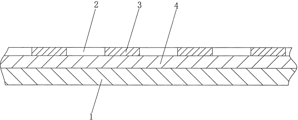
[0017] refer to figure 1 , the conductive transparent laminate body, including a transparent substrate 1 and a transparent conductive layer 2 stacked on the transparent substrate 1, the transparent conductive layer is etched into a specific pattern 3, characterized in that: the transparent substrate 1 and the transparent conductive layer A transparent buffer layer 4 with an elastic modulus of 10-30 GPa and a thickness of 1-10 μm is laid between the two.
[0018] In addition, the preferred modulus of elasticity of the transparent buffer layer 4 is 10-20 GPa, and the preferred thickness of the transparent buffer layer is 2-4 μm. The thickness of the transparent conductive layer 2 is 10-30 nm, preferably 20-25 nm. The thickness of the transparent substrate 1 is 2-300 μm, preferably 10-250 μm. The material of the transparent buffer layer 4 is acrylic resin or hardened acrylic resin, and is laid by a wet coating method of roller coating or spin coating. The material of the trans...
PUM
| Property | Measurement | Unit |
|---|---|---|
| modulus | aaaaa | aaaaa |
| thickness | aaaaa | aaaaa |
| modulus | aaaaa | aaaaa |
Abstract
Description
Claims
Application Information