Array substrate, display panel and display device and driving method thereof

A technology for array substrates and display panels, applied in static indicators, nonlinear optics, instruments, etc., can solve problems such as voltage ripple (ripple, display color shift, etc.)

Inactive Publication Date: 2016-04-13
BOE TECH GRP CO LTD +1
View PDF6 Cites 10 Cited by
  • Summary
  • Abstract
  • Description
  • Claims
  • Application Information

AI Technical Summary

Problems solved by technology

During the time of line blanking and field blanking, the loads of the gate drive circuit and the source drive circuit are suspended, and when the next frame is displayed, the first gate line is scanned and the data voltage is supplied to the first row of pixel units Signal, the gate drive circuit and the source drive circuit have a certain load, and a sudden change in the load will cause ripples in the voltage output to the pixel unit, which will cause color shift in the display screen

Method used


Image

  • Array substrate, display panel and display device and driving method thereof
  • Array substrate, display panel and display device and driving method thereof
  • Array substrate, display panel and display device and driving method thereof

Examples


Embodiment Construction

[0025] Specific embodiments of the present invention will be described in detail below in conjunction with the accompanying drawings. It should be understood that the specific embodiments described here are only used to illustrate and explain the present invention, and are not intended to limit the present invention.

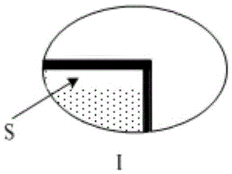
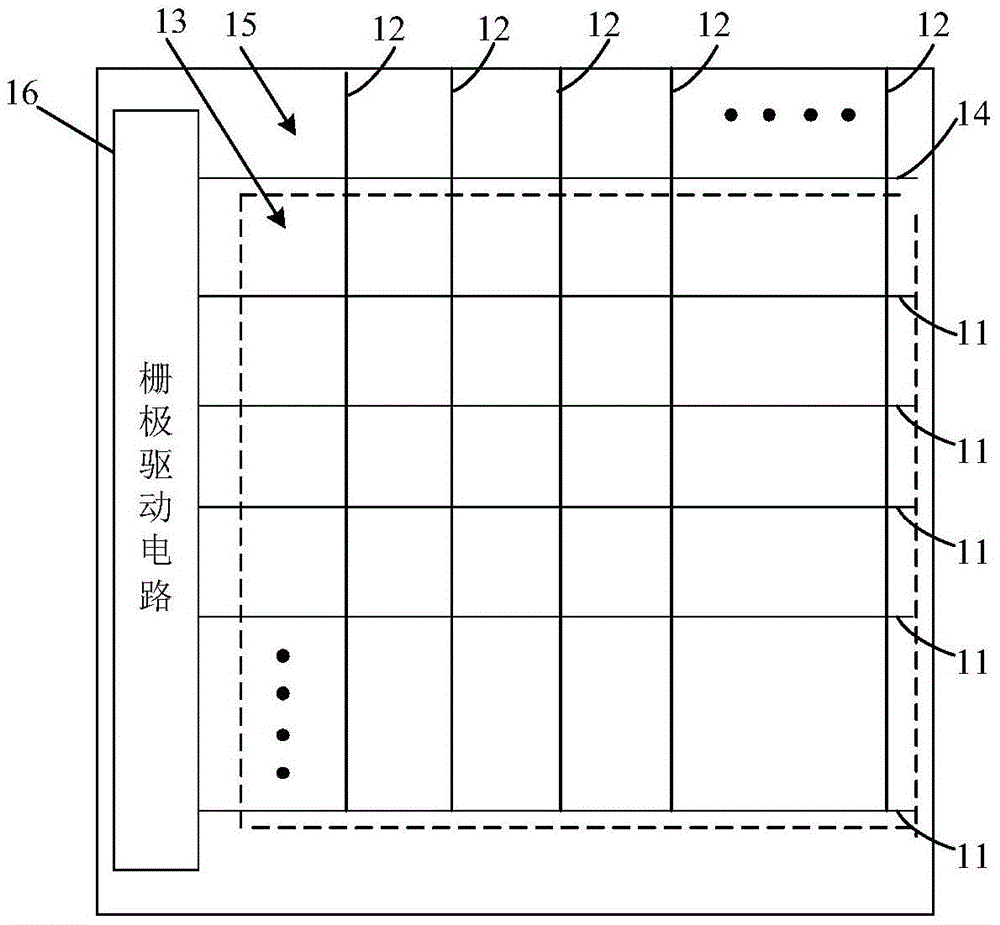
[0026] As a first aspect of the present invention, an array substrate is provided, such as image 3 As shown, the array substrate includes a display area (ie image 3 The area within the dotted line frame) and the non-display area around the display area ( image 3 The area outside the middle dotted frame), the display area is provided with a plurality of gate lines 11 and a plurality of data lines 12, and the gate lines 11 and data lines 12 intersect each other to divide the display area into a plurality of display pixel units 13 , the array substrate further includes at least one row of supplementary pixel units 15 arranged in the non-display area, and the s...


PUM


Abstract

The invention provides an array substrate, a display panel and a display device and a driving method thereof. The array substrate comprises a display area and a non-display area located at the periphery of the display area; the display area is provided with multiple grating lines and multiple data lines, and the grating lines and the data lines mutually intersect to divide the display area into multiple rows of display pixel units; the array substrate further comprises at least one row of supplementary pixel units which are arranged in the non-display area and used for receiving driving signals corresponding to the supplementary pixel units before the display pixel units receive corresponding driving signals. Accordingly, the color cast problem can be solved, and the display effect can be improved.

Description

technical field [0001] The present invention relates to the field of display technology, in particular to an array substrate, a display panel, a display device and a driving method thereof. Background technique [0002] When the display panel is displaying, the gate drive circuit sequentially provides scanning signals to each gate line on the array substrate. For two adjacent gate lines, after the scanning of the first row of gate lines is completed, the row blanking time (V -blankingtime) to start scanning the second row of grid lines. During the scanning of each gate line, the source drive circuit provides data voltage signals to each data line. After the output of the last group of data signals is completed, the next frame starts again after the vertical blanking time (H-blanking time) data output. During the time of line blanking and field blanking, the loads of the gate drive circuit and the source drive circuit are suspended, and when the next frame is displayed, the...

Claims


Application Information

Patent Timeline
Patent Type & Authority Applications(China)
IPC IPC(8): G02F1/1362G09G3/36
CPCG02F1/1362G09G3/3607G09G3/20G09G3/3648G09G2300/0413G09G2300/043G09G2300/08G09G2320/0233
Inventor 潘艳姣刘晓鹏马韬
Owner BOE TECH GRP CO LTD
Why Eureka
Try Eureka