Gate drive circuit, array substrate and display device

A gate drive circuit and circuit technology, applied in the fields of gate drive circuits, array substrates and display devices, can solve the problems of poor turn-off capability of thin film transistors of pixel units and inability to pull down gate lines quickly, so as to ensure fast pull-down, improve the turn-off capability and the effect of the

CN106409211AActive Publication Date: 2017-02-15SHANGHAI TIANMA MICRO ELECTRONICS CO LTD +1
4 Cites 6 Cited by

Patent Information

Authority / Receiving Office
CN · China
Patent Type
Applications(China)
Current Assignee / Owner
Publication Date
2017-02-15

Smart Images

  • Figure 1
    Figure 1
  • Figure 2
    Figure 2
  • Figure 3
    Figure 3
Patent Text Reader

Abstract

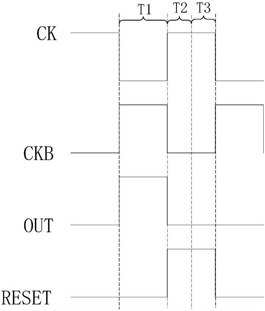
The invention provides a gate drive circuit, an array substrate and a display device. Under the control of a signal inputted by an input terminal, a shift register transmits a clock signal of a first electrical level inputted by a second clock signal terminal to an output terminal in the first period of time, and transmits a clock signal of a second electrical level inputted by the second clock signal terminal to the output terminal in the second period of time. Under the control of a signal inputted by a first clock signal terminal, the shift register transmits a pull-down signal of the second electrical level to the output terminal in the second and third periods of time. Under the control of a signal inputted by a first reset terminal, the shift register stops transmitting the clock signal inputted by the second clock signal terminal to the output terminal in the third period of time. On this basis, the electric potential of a gate line can be pulled down together by the clock signal of the second electrical level and the pull-down signal of the second electrical level in the second period of time. Therefore, fast pulldown of the gate line is guaranteed and the power-off capability of a thin film transistor of a pixel unit and the charging capability of the pixel unit are further improved.
Need to check novelty before this filing date? Find Prior Art

Description

technical field

[0001] The present invention relates to the technical field of display devices, and more specifically, to a gate drive circuit, an array substrate and a display device. Background technique

[0002] An existing display panel includes a plurality of gate lines, a plurality of data lines, a plurality of pixel units, a gate driving circuit and a data driving circuit. Wherein, the gate drive circuit includes a plurality of shift registers, the output end of each shift register is connected to a gate line, and the data drive circuit is connected to a plurality of data lines. The gate driving circuit is used for sequentially outputting scanning signals to a plurality of gate lines, and the data driving circuit is used for outputting data driving signals to the data lines to drive the pixel units to display images.

[0003] In the process of scanning the pixel units row by row, the shift register first inputs the scan signal to the gate line connected to the pixel ...

Examples

Embodiment Construction

[0029] As mentioned in the background art, the existing shift register cannot quickly pull down the potential of the gate line, which results in poor turn-off capability of the thin film transistor of the pixel unit, thereby affecting the charging capability and display effect of the pixel unit.

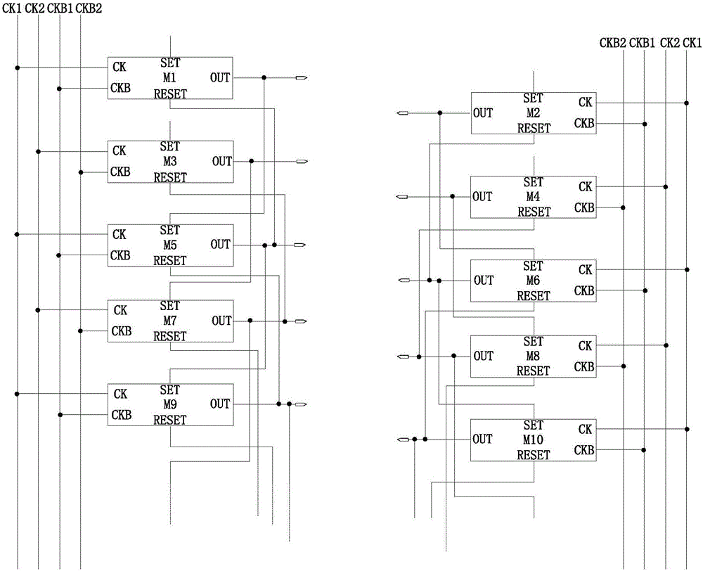
[0030] refer to figure 1 , figure 1 It is a structural schematic diagram of an existing gate driving circuit, and the gate driving circuit includes a plurality of cascaded shift registers. Among the two adjacent shift registers, the first clock signal terminal CK of one shift register is connected to the first clock signal line CK1, the second clock signal terminal CKB is connected to the second clock signal line CKB1, and the other shift register The first clock signal terminal CK of the bit register is connected to the third clock signal line CK2, and the second clock signal terminal CKB is connected to the fourth clock signal line CKB2.

[0031] Moreover, the output terminal OUT...