Voltage absorption circuit

A technology for absorbing circuits and voltages, applied in the field of circuits, can solve problems such as unfavorable electromagnetic compatibility and lower power conversion efficiency, and achieve the effect of improving energy conversion efficiency and improving EMI

Active Publication Date: 2017-04-26
TCL CHINA STAR OPTOELECTRONICS TECH CO LTD
View PDF4 Cites 0 Cited by
  • Summary
  • Abstract
  • Description
  • Claims
  • Application Information

AI Technical Summary

Problems solved by technology

[0003] At present, it is mainly through connecting a capacitor and a resistor in parallel in the rectifier diode, but the capacitor will also consume the parasitic energy while

Method used


Image

  • Voltage absorption circuit
  • Voltage absorption circuit
  • Voltage absorption circuit

Examples


Example Embodiment

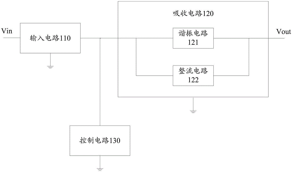
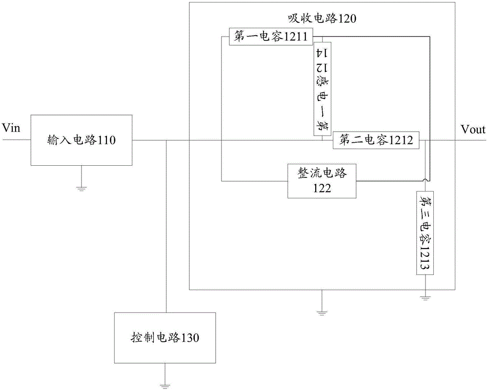
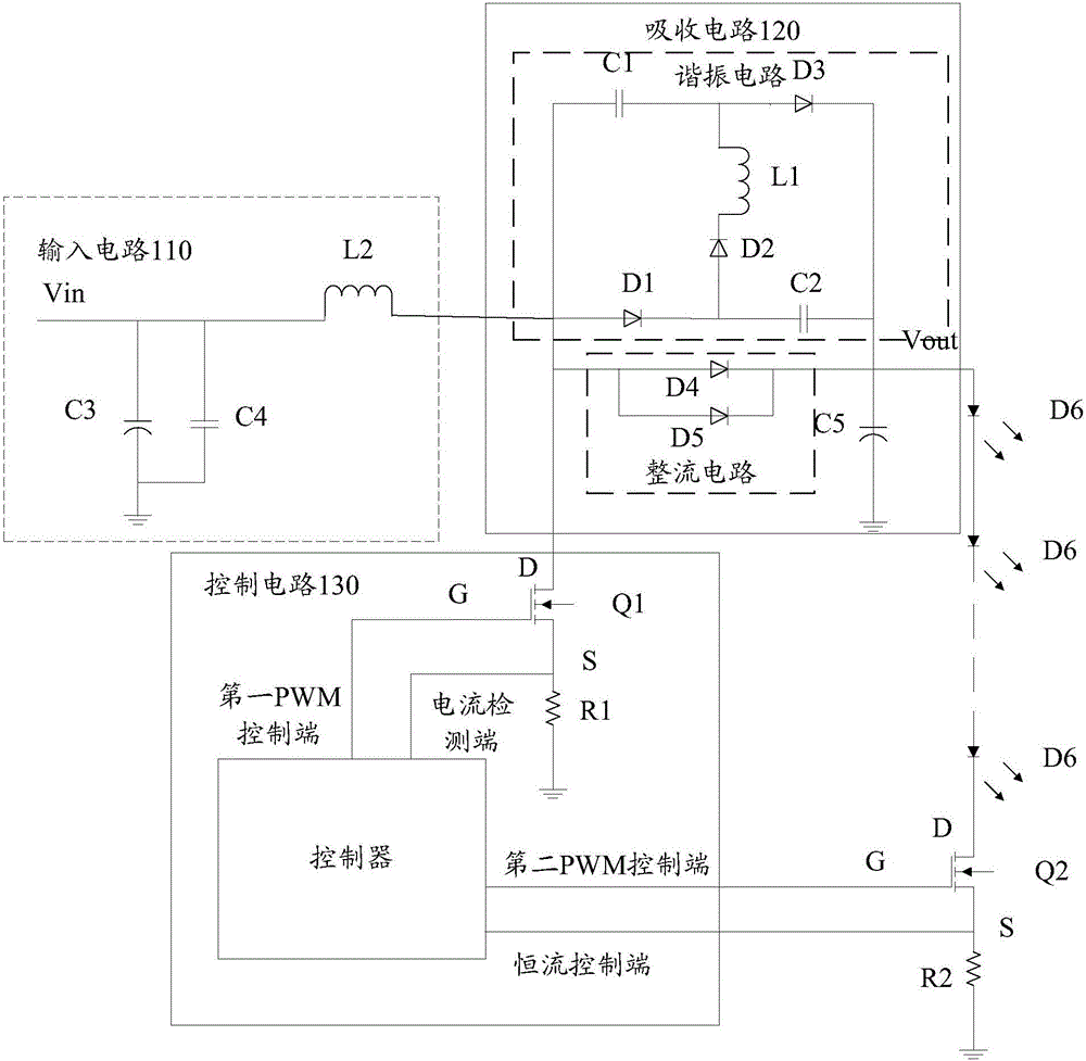
[0024] The embodiment of the present invention provides a voltage absorption circuit, in order to absorb the peak voltage losslessly, improve the energy utilization rate, and improve the EMI.

[0025] In order to enable those skilled in the art to better understand the solutions of the present invention, the technical solutions in the embodiments of the present invention will be described clearly and completely with reference to the accompanying drawings in the embodiments of the present invention. Obviously, the described embodiments are only It is a part of the embodiments of the present invention, not all the embodiments. Based on the embodiments of the present invention, all other embodiments obtained by those of ordinary skill in the art without creative work shall fall within the protection scope of the present invention.

[0026] The terms "first", "second", and "third" in the specification and claims of the present invention and the above-mentioned drawings are used to dist...


PUM


Abstract

The invention discloses a voltage absorption circuit comprising an input circuit, an absorption circuit and a control circuit, wherein the absorption circuit comprises a resonance circuit and a rectification circuit that are connected with each other in parallel. An input end of the input circuit is used for receiving input voltage; an output end of the input circuit is connected with an input end of the resonance circuit, an input end of the rectification circuit and a control end of the control circuit; the input circuit is used for providing input voltage for the voltage absorption circuit, the resonance circuit is used for absorbing peak voltage which is generated by the rectification circuit when the control circuit is switched from an off state to an on state, and the resonance circuit is also used for absorbing peak voltage which is generated when the control circuit is switched from the on state to the off state. Via adoption of the voltage absorption circuit, the peak voltage can be absorbed in a lossless manner, and energy conversion efficiency can be improved.

Description

technical field [0001] The invention relates to the field of circuits, in particular to a voltage absorbing circuit. Background technique [0002] In a TV power backlight drive circuit or a flyback circuit, when the circuit is controlled by a metal oxide semiconductor (MOS) transistor, when the MOS is turned off instantly, due to the influence of parasitic capacitance in the circuit, A turn-off peak voltage will be generated in the rectifier diode, so the peak voltage needs to be absorbed. [0003] At present, it is mainly through connecting a capacitor and a resistor in parallel in the rectifier diode, but the capacitor will also consume the parasitic energy while absorbing the peak voltage, reducing the power conversion efficiency, and is not conducive to improving the electromagnetic compatibility (Electromagnetic Interference, EMI) . Contents of the invention [0004] The embodiment of the present invention provides a voltage absorbing circuit, in order to absorb pea...

Claims


Application Information

Patent Timeline
IPC IPC(8): H02H9/04H04N5/63
CPCH02H9/045H04N5/63
Inventor 李文东
Owner TCL CHINA STAR OPTOELECTRONICS TECH CO LTD
Why Eureka
Try Eureka