FPGA development board and communication method thereof

A development board and communication module technology, applied in the FPGA field, can solve problems such as unusable download debugger, incompatible drivers, lengthy and complicated process, etc., to improve user experience and ease of use, reduce learning difficulty, and improve learning efficiency Effect

Active Publication Date: 2017-12-29
苏州思得普信息科技有限公司
View PDF2 Cites 5 Cited by
  • Summary
  • Abstract
  • Description
  • Claims
  • Application Information

AI Technical Summary

Problems solved by technology

[0010] Due to the large size of the current download debugger hardware, it is used separately from the development board. Every time you use it, you need to use a USB cable and a flat cable to connect the computer and the development board, which is inconvenient to use.
[0011] The download debugger uses the USB interface to communicate. The USB module must be used with the FPGA development software of major FPGA manufacturers. The driver program of the manufacturer must be installed. Due to the different compatibility of the operating system, the driver is often incompatible, resulting in download debugging. unavailable
[0012] During the download process, the FPGA software will verify the ID information of the FPGA chip, and then decode, download, and verify the file. The whole process is lengthy and complicated, resulting in slow download speed and poor user experience.
The download debugger generally uses an expensive dedicated USB conversion chip, and also requires a CPLD chip, resulting in a high hardware cost for the entire downloader

Method used


Image

  • FPGA development board and communication method thereof
  • FPGA development board and communication method thereof
  • FPGA development board and communication method thereof

Examples


Embodiment Construction

[0032] In order to make the object, technical solution and advantages of the present invention clearer, the present invention will be further described in detail below in conjunction with the accompanying drawings and embodiments. It should be understood that the specific embodiments described here are only used to explain the present invention, not to limit the present invention.

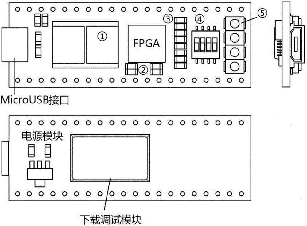
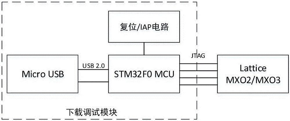
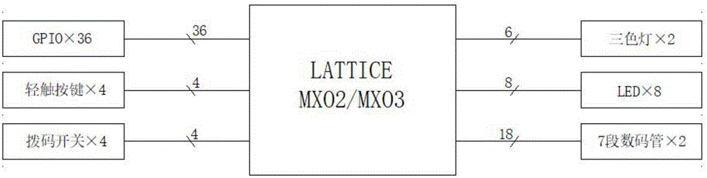
[0033] refer to figure 1 , an FPGA development board, comprising: a Micro USB interface, a power supply module, an FPGA core chip, a peripheral module and a downloading and debugging module connected to the FPGA core chip.

[0034] The development board uses the Micro USB interface as the power supply interface and USB communication interface of the entire board. The USB power supply is input to the power module, and the voltage of +3.3V is output through the low-dropout linear regulator to supply power to all modules of the board.

[0035] In another embodiment, the FPGA core chip adopts the MXO...


PUM


Abstract

The invention relates to an FPGA development board. The FPGA development board comprises a Micro USB interface, a power module, an FPGA core chip and a peripheral module. The FPGA development board also comprises a downloading debugging module connected with the FPGA core chip, wherein the downloading debugging module comprises a communication module, a master controller and a peripheral circuit; the master controller is connected with the communication module and the peripheral circuit; and the communication module is provided with a USB2.0 interface. Through the FPGA development board, the learning difficulty of a user is lowered, the learning efficiency of the user is improved, the size of the FPGA development board is reduced, and user experience and usability are improved. The invention furthermore relates to a communication method of the FPGA development board.

Description

technical field [0001] The present invention relates to FPGA, in particular to FPGA development board and communication method thereof. Background technique [0002] Programmable logic technology: FPGA (Field-Programmable Gate Array, Field Programmable Logic Gate Array), is a product of further development in the field of digital logic based on PAL, GAL, CPLD and other technologies, and ASIC (Application-specific integrated circuit , application-specific integrated circuits) complement each other, overcome the problem that ASIC is not flexible enough as a custom circuit, and also solve the shortage of logic resources of GAL, CPLD and other devices. At the same time, more importantly, FPGA is an important tool in the chip verification process. Because of this, since FPGA entered the country, it has been highly valued, and the country's investment in this industry has also increased year by year. In order to open up the market and expand the market share of FPGA, FPGA manufac...

Claims


Application Information

Patent Timeline
Patent Type & Authority Applications(China)
IPC IPC(8): G06F9/445G06F13/10G06F13/38
CPCG06F8/654G06F13/102G06F13/385
Inventor 陈强吴志军王安然张泽高尚
Owner 苏州思得普信息科技有限公司
Why Eureka
Try Eureka