Array substrate and display panel

一种阵列基板、显示区的技术,应用在仪器、半导体器件、计算等方向,能够解决制约显示面板边框区缩小等问题,达到减小面积、缩小边框面积的效果

CN107783698AActive Publication Date: 2018-03-09SHANGHAI TIANMA MICRO ELECTRONICS CO LTD +1
7 Cites 14 Cited by

Patent Information

Authority / Receiving Office
CN · China
Patent Type
Applications(China)
Current Assignee / Owner
Publication Date
2018-03-09

Smart Images

  • Figure 1
    Figure 1
  • Figure 2
    Figure 2
  • Figure 3
    Figure 3
Patent Text Reader

Abstract

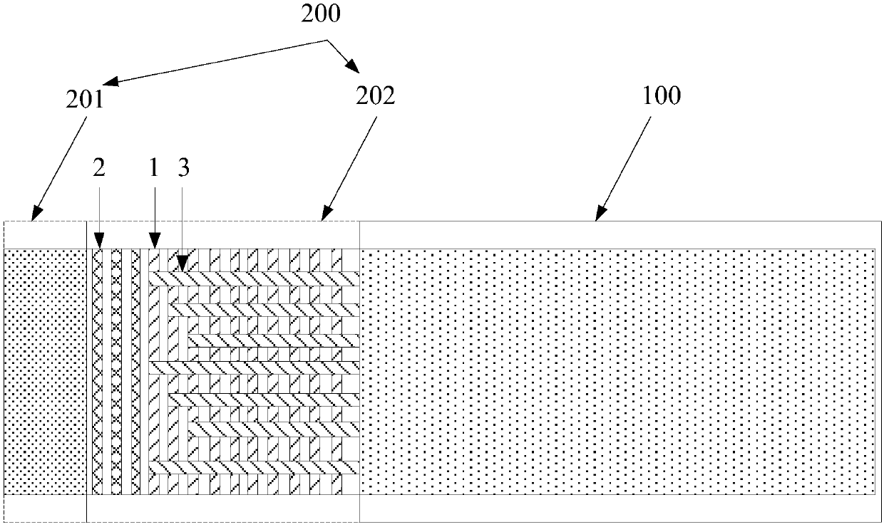
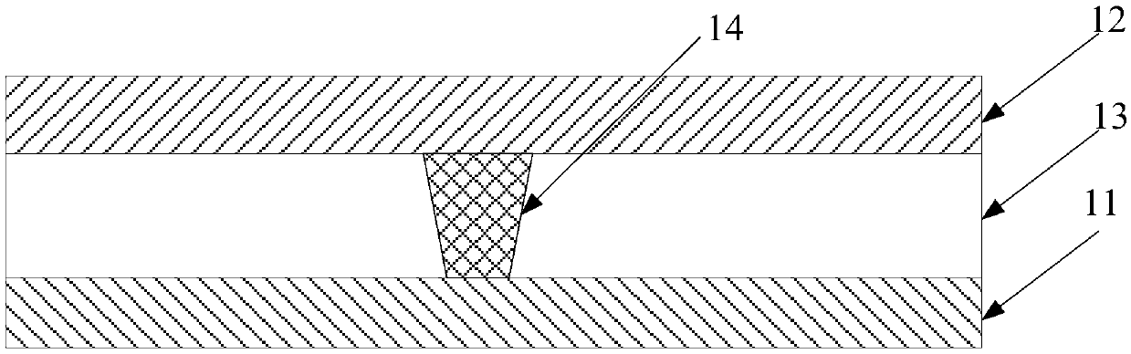
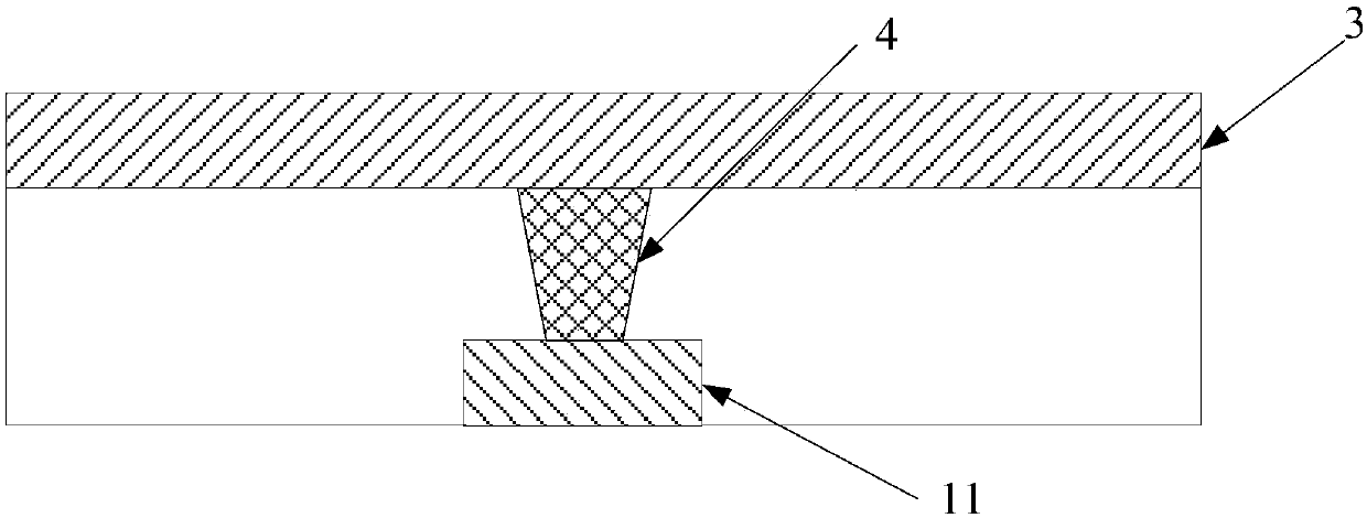
The embodiment of the invention discloses an array substrate and a display panel. The array substrate comprises a display area and a frame area, wherein the frame area comprises a driving circuit areaand a wire distributing area used for connecting the driving circuit area with the display area; the wire distributing area comprises a first signal wire layer and a second signal wire layer which are successively overlapped and a first insulation layer located between the first signal wire layer and the second signal wire layer; the first signal wire layer comprises a plurality of first signal wires extending along a first direction; the second signal wire layer comprises a plurality of second signal wires extending along the first direction; the first signal wires and the second signal wires are at least partially overlapped along a direction vertical to the surface of the array substrate. According to the array substrate and the display panel, the first signal wires and the second signal wires are overlapped, so that the area of the wire distributing area in the array substrate is reduced, and then the frame area of the display panel comprising the array substrate is reduced.
Need to check novelty before this filing date? Find Prior Art

Description

[0001] This application is a divisional application with an application date of April 1, 2015, an application number of 201510152796.7, and an invention titled "an array substrate and its manufacturing method, and a display panel". technical field

[0002] The present invention relates to the technical field of touch display, in particular to an array substrate, a manufacturing method thereof, and a display panel including the array substrate. Background technique

[0003] With the development of display technology, more and more display panels are integrated with touch function, and its touch principle is divided into mutual capacitance touch technology and self-capacitance touch technology, wherein, the self-capacitance touch technology is due to The mutual capacitance touch technology only needs one layer of touch electrodes, which is more suitable for the development of thinner and thinner display panels. At the same time, under the limited size of the display panel, how...

Examples

Embodiment Construction

[0052] The following will clearly and completely describe the technical solutions in the embodiments of the present invention with reference to the accompanying drawings in the embodiments of the present invention. Obviously, the described embodiments are only some, not all, embodiments of the present invention. Based on the embodiments of the present invention, all other embodiments obtained by persons of ordinary skill in the art without making creative efforts belong to the protection scope of the present invention.

[0053] In the following description, a lot of specific details are set forth in order to fully understand the present invention, but the present invention can also be implemented in other ways different from those described here, and those skilled in the art can do it without departing from the meaning of the present invention. By analogy, the present invention is therefore not limited to the specific examples disclosed below.

[0054] An embodiment of the pre...