Array substrate, as well as drive method and drive circuit of array substrate, and display device

A technology of an array substrate and a driving method, which is applied to circuits, electrical components, static indicators, etc., can solve problems such as abnormal screens of display devices, and achieve the effect of solving abnormal screens and improving display effects

Active Publication Date: 2018-04-24
BOE TECH GRP CO LTD
View PDF5 Cites 8 Cited by
  • Summary
  • Abstract
  • Description
  • Claims
  • Application Information

AI Technical Summary

Problems solved by technology

[0005] The technical problem to be solved by the present invention is to provide an array substrate and its driving method, driving circuit and display device, which can solve the problem of abnormal screen of the display device and improve the display effect of the display device

Method used


Image

  • Array substrate, as well as drive method and drive circuit of array substrate, and display device
  • Array substrate, as well as drive method and drive circuit of array substrate, and display device
  • Array substrate, as well as drive method and drive circuit of array substrate, and display device

Examples


Embodiment Construction

[0034] In order to make the technical problems, technical solutions and advantages to be solved by the embodiments of the present invention clearer, the following will describe in detail with reference to the drawings and specific embodiments.

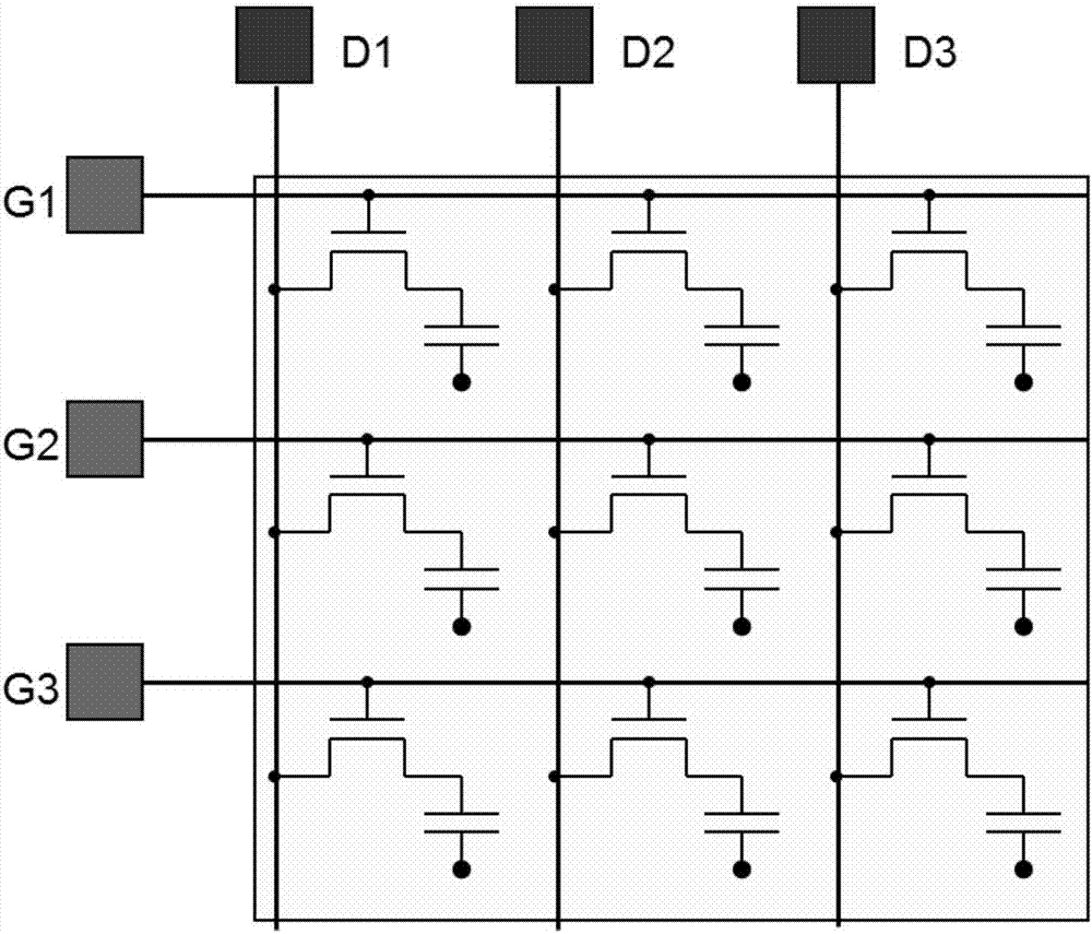
[0035] In the existing technology, such as figure 1 As shown, each sub-pixel area is provided with a switch thin film transistor, and in the display period of one frame, the gate electrode of the metal oxide thin film transistor is switched off after receiving the gate scanning signal. When the gate of the metal oxide thin film transistor is connected to the low level for a long time, the metal oxide thin film transistor will be negatively biased, and the threshold voltage will shift to the left.

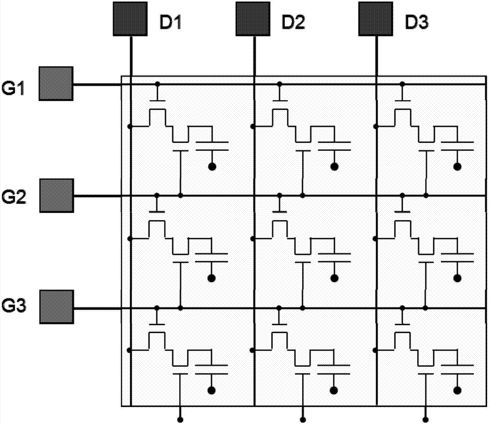
[0036] In order to solve the above problems, embodiments of the present invention provide an array substrate and its driving method, a driving circuit, and a display device, which can solve the problem of abnormal screen of the display devic...


PUM


Abstract

The invention provides an array substrate, as well as a drive method and a drive circuit of the array substrate, and a display device, belonging to the technical field of display. The array substratecomprises a plurality of grid lines and a plurality of data lines in crossed distribution, the grid lines and the data lines define a plurality of sub-pixel areas, a switch thin film transistor and apixel electrode are formed in each sub-pixel area, each sub-pixel area is provided with a plurality of switch thin film transistors, the grid electrodes of the plurality of switch thin film transistors are connected with different grid lines, and the plurality of switch thin film transistors are used for transmitting data voltage signals to the pixel electrodes when signals of the grid lines connected with the grid electrodes of the plurality of switch thin film transistors are at effective levels. With the technical scheme, the problem that a picture of a display device is abnormal can be solved, and the display effect of the display device can be improved.

Description

technical field [0001] The present invention relates to the field of display technology, in particular to an array substrate, a driving method thereof, a driving circuit and a display device. Background technique [0002] In recent years, with the rapid development of display technology, thin film transistors for driving and controlling pixels have also been developed, from amorphous silicon thin film transistors and low temperature polysilicon thin film transistors to metal oxide thin film transistors. [0003] Metal oxide thin film transistors are excellent in characteristics such as electron mobility, on-state current, and switching characteristics. In addition, the metal oxide thin film transistor also has the advantages of less uneven characteristics, low material and process costs, low process temperature, available coating process, high light transmittance, and large band gap. Therefore, metal oxide thin film transistors can be used in displays that require fast resp...

Claims


Application Information

Patent Timeline
Patent Type & Authority Applications(China)
IPC IPC(8): G09G3/36G09G3/20
CPCG09G3/20G09G3/3648G09G3/3225G09G3/36G09G2310/0205G09G2320/043G09G2300/0404G02F1/13624G02F1/1368G02F2202/10G09G3/3677G09G3/3688G09G2300/0426G09G2300/0819G09G2310/021G09G2320/045H01L27/1225H01L27/124H01L29/7869
Inventor 韩承佑商广良
Owner BOE TECH GRP CO LTD
Why Eureka
Try Eureka