Circuit for accessing chip test mode and control method of circuit

A chip test and test mode technology, applied in the direction of measuring electricity, measuring electrical variables, digital circuit testing, etc., can solve problems such as complex operation, waste of pin resources, affecting test coverage, etc., to achieve strong operability and simple circuit , The entry method is simple and controllable

Pending Publication Date: 2018-08-17
AMICRO SEMICON CORP
View PDF15 Cites 11 Cited by
  • Summary
  • Abstract
  • Description
  • Claims
  • Application Information

AI Technical Summary

Problems solved by technology

The operation of these test methods is relatively complicated, and there is a large waste of pin resources, which also affects the coverage of the test.

Method used


Image

  • Circuit for accessing chip test mode and control method of circuit
  • Circuit for accessing chip test mode and control method of circuit
  • Circuit for accessing chip test mode and control method of circuit

Examples


Embodiment approach

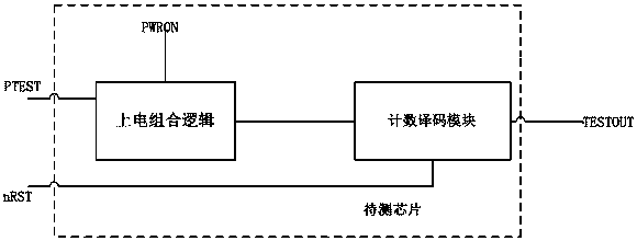
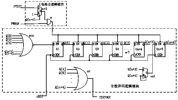
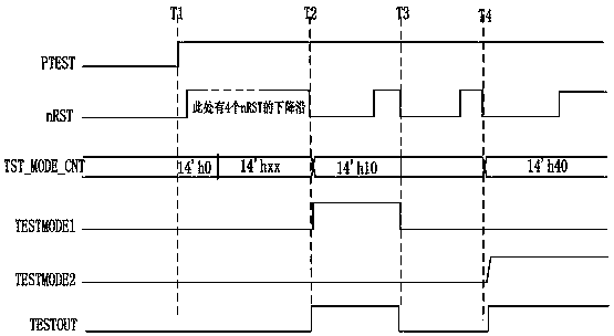
[0052] As an embodiment of the present invention, the control method further includes a method of exiting the chip test mode, which includes, after the chip to be tested enters the current chip test mode, the counting and decoding module passes the reset input Terminal nRST receives a falling edge signal, then the chip to be tested exits the current chip test mode, and waits until the reset input terminal nRST receives the next falling edge signal, then the chip to be tested enters the next chip test mode ;

[0053] When the chip to be tested has entered the chip test mode and is being tested, the chip to be tested is forcibly exited from the chip test mode by inputting a low level to the test mode enable input terminal PTEST. When the test mode enable input terminal PTEST keeps low level, the settings of the chip test mode are cleared, but the scan test mode is not affected by it.

[0054] As an embodiment of the present invention, the control method further includes a contr...


PUM


Abstract

The invention relates to a circuit for accessing a chip test mode and a control method of the circuit. The circuit comprises a power-on reset logic module and a counting decoding logic module, an existing chip pin is reused, the counting decoding logic module based on one-hot encoding counting is designed to access and switch various test modes, pin sources of a chip are saved, test efficiency ofthe chip is improved, chip test is in a scan chain test mode when clock jump is driven, and the test coverage rate of a scan chain can be increased.

Description

technical field [0001] The invention relates to the field of chip testing, in particular to a circuit for entering a chip testing mode and a control method thereof. Background technique [0002] In modern chip design, the success of a chip is closely related to the testability of the chip. At the same time, chip testing is also an important part of chip cost. A good chip testing method can greatly save the cost of chip testing. On the contrary, if the chip testing cost is high, it will directly increase the cost of the chip, which is not conducive to the chip participating in the fierce market competition. Therefore, many chips have made detailed plans for chip testing at the beginning of the project. [0003] In the current technology, many chip test circuits require a special chip configuration or allow the chip to be tested to set aside special pins to complete the design of the chip test mode. The operation of these test methods is relatively complicated, there is a l...

Claims


Application Information

Patent Timeline
IPC IPC(8): G01R31/3185G01R31/317
CPCG01R31/31718G01R31/3172G01R31/318536G01R31/318555G01R31/318583Y02D10/00
Inventor 何再生
Owner AMICRO SEMICON CORP
Why Eureka
Try Eureka