Array substrate, display panel and display device

An array substrate and display area technology, which is applied in the fields of display panels, display devices, and array substrates, can solve the problems of large difference in the load of data connection leads and affect the quality of display images, and can reduce height, reduce load difference, and improve quality. Effect

Active Publication Date: 2022-05-20
XIAMEN TIANMA MICRO ELECTRONICS
View PDF6 Cites 0 Cited by
  • Summary
  • Abstract
  • Description
  • Claims
  • Application Information

AI Technical Summary

Problems solved by technology

In the prior art, the data connection leads are usually located on the first metal layer (the film layer where the scan line is located) and the second metal layer (the film layer where the source and drain electrodes are located), wherein the coupling capacitance between two adjacent data connection leads is relatively small. Large, resulting in a large difference in the load on two adjacent data connection leads, affecting the quality of the display screen

Method used


Image

  • Array substrate, display panel and display device
  • Array substrate, display panel and display device
  • Array substrate, display panel and display device

Examples


Embodiment Construction

[0029] The present invention will be further described in detail below in conjunction with the accompanying drawings and embodiments. It should be understood that the specific embodiments described here are only used to explain the present invention, but not to limit the present invention. In addition, it should be noted that, for the convenience of description, only some structures related to the present invention are shown in the drawings but not all structures.

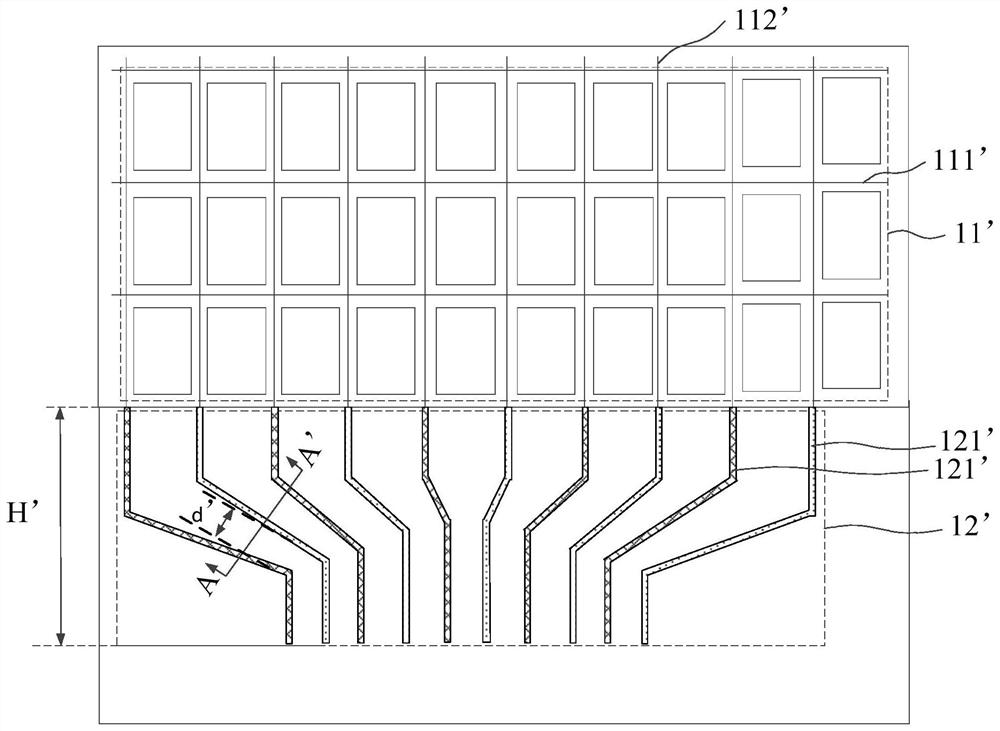
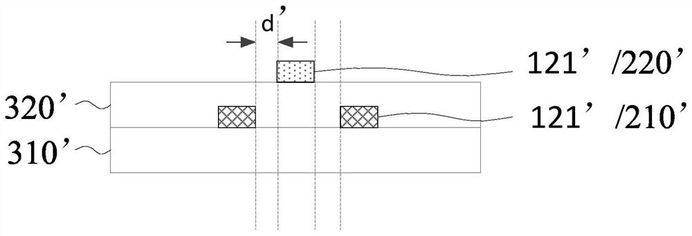
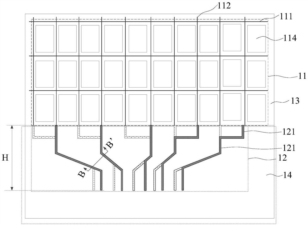
[0030] figure 1 It is a structural schematic diagram of an array substrate provided in the prior art. figure 2 yes figure 1 Schematic diagram of the cross-sectional structure along the direction AA'. see figure 1 with figure 2 , the display panel includes a display area 11' and a fan-out area 12'; it also includes: a base substrate 310', and a first metal layer 210' located on one side of the base substrate 310'; the first metal layer 210' is used in the display A plurality of scanning lines 111' are formed...


PUM


Abstract

The embodiment of the invention discloses an array substrate, a display panel and a display device. Including: a base substrate, a first metal layer, an interlayer dielectric layer, a second metal layer, an organic planarization layer and a third metal layer; the first metal layer forms a plurality of scanning lines in the display area, and does not form in the fan-out area Data connection leads; the second metal layer forms a plurality of data lines in the display area, and forms a plurality of data connection leads in the fan-out area; the third metal layer forms a plurality of data connection leads in the fan-out area; wherein, the data connection leads are adjacent to the display One end of the region is electrically connected to the data lines in one-to-one correspondence; two adjacent data connection leads are located in different layers, and the vertical projections on the base substrate are at least partially overlapped. The technical solution provided by the embodiment of the present invention can reduce the load difference on two adjacent data connection leads, and at the same time, can also reduce the height of the fan-out area.

Description

technical field [0001] Embodiments of the present invention relate to the field of display technology, and in particular, to an array substrate, a display panel, and a display device. Background technique [0002] With the development of display technology, liquid crystal displays and organic light-emitting displays have become the two mainstream products in the display field. At the same time, consumers' performance requirements for displays are also constantly improving. [0003] The display usually includes a display area and a frame area surrounding the display area. The display area includes a plurality of scanning lines and a plurality of data lines intersecting each other, and a plurality of scanning lines and a plurality of data lines intersect to define a plurality of sub-pixel units; the frame area includes a lower frame area, the lower frame area includes a plurality of data connection leads, the data connection leads are used to electrically connect the driver ch...

Claims


Application Information

Patent Timeline
Patent Type & Authority Patents(China)
IPC IPC(8): G02F1/1362G02F1/1345G02F1/1333H01L27/32
CPCG02F1/136286G02F1/13452G02F1/1333G02F1/13338G02F1/133357G02F1/13629H10K59/40H10K59/131
Inventor 魏晓丽李东华周秀峰沈柏平
Owner XIAMEN TIANMA MICRO ELECTRONICS
Why Eureka
Try Eureka