

Array substrate and display motherboard
A technology of array substrates and plates, which is applied to semiconductor/solid-state device parts, capacitors, semiconductor devices, etc., can solve the problems of affecting display quality, dim brightness, uneven film quality, etc., and achieve the effect of improving display quality
- Summary
- Abstract
- Description
- Claims
- Application Information
AI Technical Summary
Problems solved by technology
Method used
Image

Examples
Embodiment Construction
[0031] In order to make the purpose, technical solution and advantages of the present application clearer, the present application will be further described in detail below in conjunction with the accompanying drawings and embodiments. It should be understood that the specific embodiments described here are only used to explain the present application, and are not intended to limit the present application.
[0032] The array substrate and display motherboard provided in the present application can be applied to fabricate organic light-emitting display panels, and can also be used to fabricate other types of display panels, which is not limited in the present application.
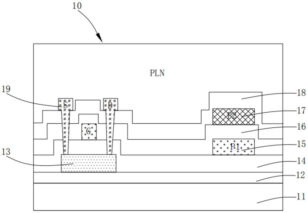
[0033] The display panel has a plurality of sub-pixels of various colors, such as a red sub-pixel R, a green sub-pixel G, and a blue sub-pixel B, and images are displayed by each sub-pixel. Display panels are usually formed after cutting a large display motherboard (a motherboard that can be cut into multipl...
PUM
| Property | Measurement | Unit |
|---|---|---|
| thickness | aaaaa | aaaaa |
Abstract
Description
Claims
Application Information