A pin automatic plug-in device for pcb board

A PCB board and pin technology, which is applied in the field of pin automatic plug-in device, can solve problems such as inability to perform batch pin welding, damage to the printed circuit of the PCB board, and pin deformation.

Active Publication Date: 2021-01-01
江西众达泰科技有限公司
View PDF11 Cites 0 Cited by
  • Summary
  • Abstract
  • Description
  • Claims
  • Application Information

AI Technical Summary

Problems solved by technology

[0007] In order to overcome the lack of soldering in the state of unclamped pins in the prior art, the present invention cannot perform batch soldering of the pins, and relies heavily on graphic positioning processing during movement, and there are sharp parts at the end of the pins, which are easy to be scratched in the subsequent welding process Injury to the staff, if there is a deviation in positioning, it is easy to damage the printed circuit on the PCB board, and the pin is easily bent from the component, and the original shape of the pin is deformed during bending, which makes the connection of the component loose Cause component damage, reduce the working life and tolerance of the components, the technical problem to be solved by the present invention is to provide an automatic pin insertion device for PCB boards

Method used


Image

  • A pin automatic plug-in device for pcb board
  • A pin automatic plug-in device for pcb board
  • A pin automatic plug-in device for pcb board

Examples


Embodiment

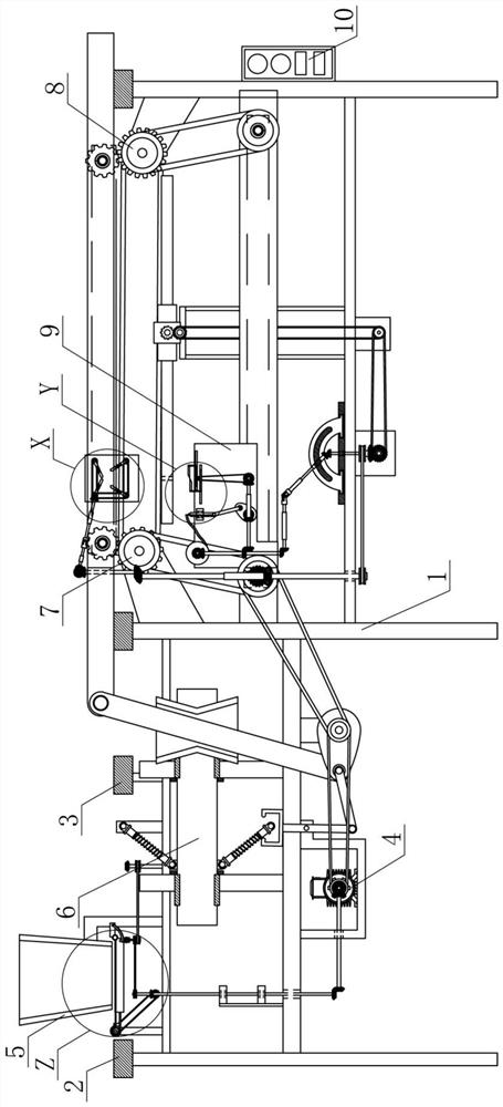
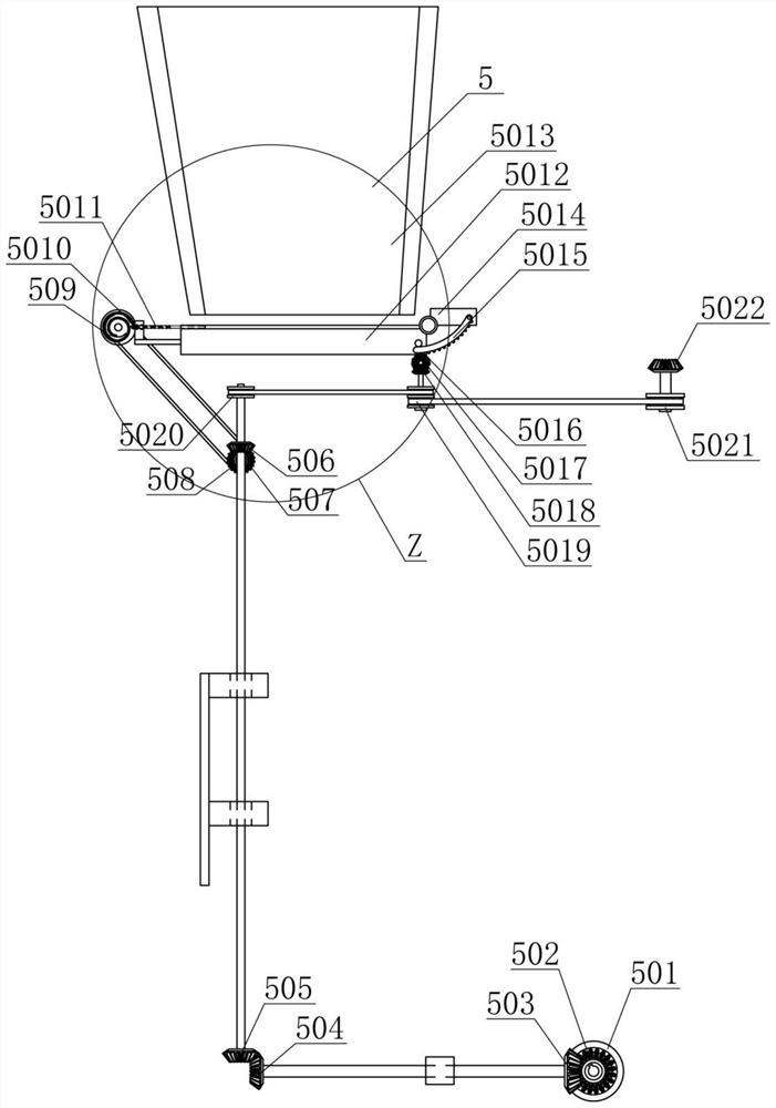
[0030] A pin automatic plug-in device of a PCB board, such as Figure 1-8As shown, it includes a fixed frame 1, a first limit block 2, a second limit block 3, a stepper motor 4, a pin standing mechanism 5, a reverse pin insertion mechanism 6, a first transmission wheel 7, and a second Transmission wheel 8, cutting and welding review mechanism 9 and controller; the top left end of fixed frame 1 is welded with first limit block 2; the left middle part of fixed frame 1 top is welded with second limit block 3; the left middle part of fixed frame 1 is welded with The stepper motor 4 is bolted; the left end of the fixed frame 1 is provided with a pin stand mechanism 5, and the bottom right of the rear end of the pin stand mechanism 5 is connected with the stepper motor 4; the left middle top of the fixed frame 1 is provided with a reverse Pin insertion mechanism 6, and the left end of reverse pin insertion mechanism 6 is connected with pin standing mechanism 5 by belt; The middle to...


PUM


Abstract

The invention relates to circuit board production, in particular to an automatic PCB pin insertion device. The technical problem to be solved by the present invention is to provide an automatic PCB pin insertion device. The automatic PCB pin insertion device includes a fixed frame, a first stopping block, a second stopping block, a stepping motor, a pin erecting mechanism, a reverse pin insertionmechanism, a first driving wheel, a second driving wheel, a cutting and soldering review mechanism and a controller. The top of the left end of the fixed frame is welded to the first stopping block. The left middle of the top of the fixed frame is welded to the second stopping block. The left middle of the fixed frame is in bolted connection with the stepping motor. The pin erecting mechanism is disposed on the left end in the fixed frame. The automatic PCB pin insertion device achieves effects of facilitating pin clamping, positioning PCB holes, shortening the pins to avoid scratching users and damaging other boards in transit, and avoiding damaging the use states of components during cutting.

Description

technical field [0001] The invention relates to a circuit board production, in particular to an automatic pin insertion device for a PCB board. Background technique [0002] PCB, the Chinese name is printed circuit board, also known as printed circuit board, is an important electronic component, a support for electronic components, and a carrier for electrical connections of electronic components. Since it is made by electronic printing, it is Known as a "printed circuit board. [0003] Prior Art Chinese patent CN109348700A aims at the problem of existing additional processes and relatively high positioning accuracy requirements, and discloses a mobile plug-in method and a plug-in device. Based on the current target jack pose, the transmission device-related Displacement information and the current pin pose, the way to generate instructions overcomes the problem of increasing the process and requiring relatively high positioning accuracy, but due to inaccurate graphic recog...

Claims


Application Information

Patent Timeline
Patent Type & Authority Patents(China)
IPC IPC(8): H05K13/04
CPCH05K13/04H05K13/0404H05K13/0406
Inventor 王录山
Owner 江西众达泰科技有限公司
Why Eureka
Try Eureka