

Wafer cleaning device
A technology for cleaning devices and wafers, applied in cleaning methods and tools, cleaning methods using tools, cleaning methods using liquids, etc., can solve problems affecting wafer quality, easily scratching wafers, and low cleaning efficiency. Achieve the effect of unaffected quality and qualified rate, clean and thorough scrubbing, and improved scrubbing efficiency
- Summary
- Abstract
- Description
- Claims
- Application Information
AI Technical Summary
Problems solved by technology
Method used
Image

Examples
Embodiment Construction
[0049] The present invention will be further described below in conjunction with specific examples. However, the uses and purposes of these exemplary embodiments are only used to illustrate the present invention, and do not constitute any form of limitation to the actual protection scope of the present invention, nor limit the protection scope of the present invention thereto.
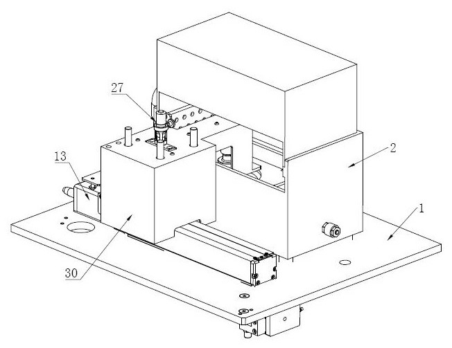
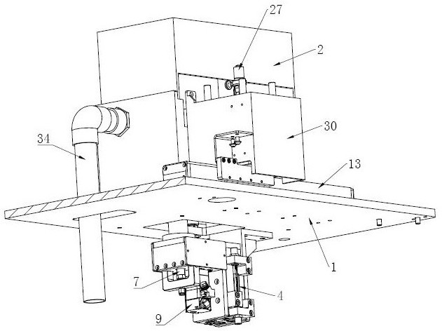
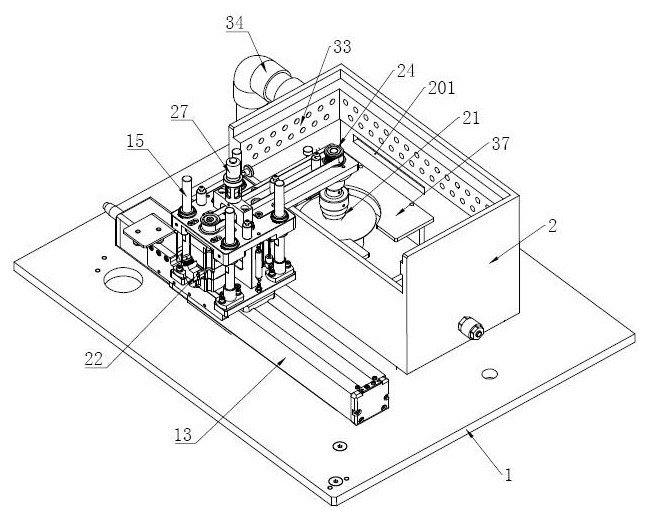
[0050] Such as Figure 1 to Figure 9 Commonly shown, this embodiment provides a wafer cleaning device, including a cleaning workbench 1, a cleaning box 2 is fixedly installed on the cleaning workbench 1, and a strip-shaped wafer pick-and-place opening is provided on one side of the cleaning box 2 201, so as to facilitate the picking and placing of wafers in the cleaning box 2.
[0051] The bottom of the cleaning workbench 1 is slidably installed with the installation frame 5 driven by the first drive device in the vertical direction, and the vacuum tube 7 driven by the second drive device is rotated o...
PUM
 Abstract
Description
Claims
Application Information