Semiconductor device and manufacturing method thereof

A semiconductor and device technology, applied in the field of semiconductor devices and their manufacturing, can solve problems such as poor marking morphology, achieve the effect of avoiding poor filling and improving the accuracy of the shape

Pending Publication Date: 2021-03-16
WUHAN XINXIN SEMICON MFG CO LTD
View PDF0 Cites 0 Cited by
  • Summary
  • Abstract
  • Description
  • Claims
  • Application Information

AI Technical Summary

Problems solved by technology

[0005] The purpose of the present invention is to provide a semiconductor device an

Method used


Image

  • Semiconductor device and manufacturing method thereof
  • Semiconductor device and manufacturing method thereof
  • Semiconductor device and manufacturing method thereof

Examples


Embodiment Construction

[0046] A semiconductor device and its manufacturing method proposed by the present invention will be further described in detail below with reference to the accompanying drawings and specific embodiments. The advantages and features of the present invention will become clearer from the following description. It should be noted that all the drawings are in a very simplified form and use imprecise scales, and are only used to facilitate and clearly assist the purpose of illustrating the embodiments of the present invention. In addition, the structures shown in the drawings are often a part of the actual structure. In particular, each drawing needs to display different emphases, and sometimes uses different scales.

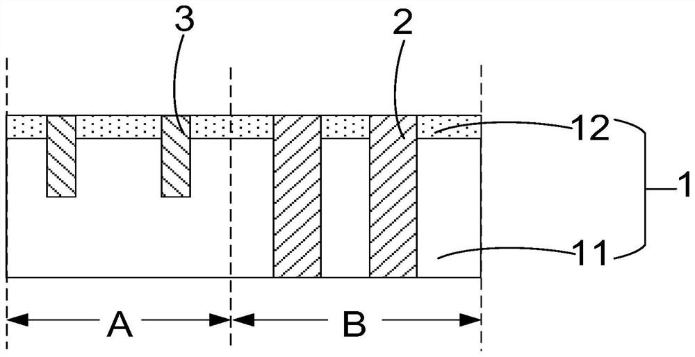
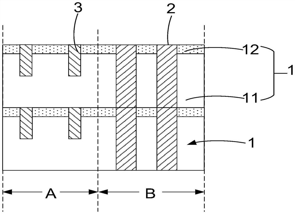
[0047] figure 1 is a schematic structural view of a semiconductor device according to an embodiment of the present invention. Such as figure 1 As shown, the present embodiment provides a semiconductor device, which includes at least one semiconductor substrate 1 ...


PUM


Abstract

The invention provides a semiconductor device and a manufacturing method thereof. When a component and a mark extending into a semiconductor substrate are formed in the same process, the maximum depthof the mark opening formed by etching is still smaller than the minimum depth of the component opening when the widths of the mark opening and the component opening are not changed; therefore, when the mark opening and the component opening are filled with the material I at the same time to form the mark and the component, the filling performance of the mark opening with smaller depth is good, and the morphology of the formed mark can be further guaranteed.

Description

technical field [0001] The invention relates to the technical field of semiconductors, in particular to a semiconductor device and a manufacturing method thereof. Background technique [0002] In the semiconductor device manufacturing process, almost every photolithography process involves the process of alignment, alignment or measurement. The so-called alignment or alignment process refers to the identification of special alignment marks on the surface of the substrate by machine recognition or human eyes on the lithography equipment, so that the back-end process and the front-end process have positional overlap. The so-called measurement process refers to identifying the marks by the machine, and then calculating information such as the position between the marks. Therefore, in the manufacturing process of semiconductor devices, marks are usually prepared on the wafer for alignment or measurement. [0003] However, in the existing manufacturing process of semiconductor ...

Claims


Application Information

Patent Timeline
IPC IPC(8): H01L23/544H01L21/308
CPCH01L23/544H01L21/308H01L2223/54426
Inventor 冯奕程黄宇恒陈帮
Owner WUHAN XINXIN SEMICON MFG CO LTD
Why Eureka
Try Eureka