An integrated semiconductor device

A semiconductor and device technology, applied in the field of integrated semiconductor devices, can solve problems such as increasing manufacturing procedures, achieve the effects of improving quality, avoiding reverse narrow channel effect, and saving process steps

Active Publication Date: 2021-05-25
晶芯成(北京)科技有限公司
View PDF4 Cites 0 Cited by
  • Summary
  • Abstract
  • Description
  • Claims
  • Application Information

AI Technical Summary

Problems solved by technology

[0003] In the manufacture of static memory, due to the unreasonable setting of the active area and the gate width, when implanting ions in the active area, in order to reach the set channel turn-on voltage, it is necessary to perform multiple ion implantations on the active area, and then It is necessary to increase the mask, reprint ion, and increase the manufacturing process

Method used


Image

  • An integrated semiconductor device
  • An integrated semiconductor device
  • An integrated semiconductor device

Examples


Embodiment Construction

[0037] The following will clearly and completely describe the technical solutions in the embodiments of the present invention with reference to the accompanying drawings in the embodiments of the present invention. Obviously, the described embodiments are only some, not all, embodiments of the present invention. Based on the embodiments of the present invention, all other embodiments obtained by persons of ordinary skill in the art without creative efforts fall within the protection scope of the present invention.

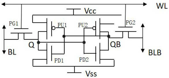
[0038] The present invention provides an integrated semiconductor device, the semiconductor integrated device is a static random access memory, the equivalent circuit diagram of the static random access memory is as follows figure 1 As shown, it includes two drive transistors, the first drive transistor PD1 and the second drive transistor PD2, two load transistors, the first load transistor PU1 and the second load transistor PU2, and two pass transistors, the first ...


PUM


Abstract

The invention discloses an integrated semiconductor device, which includes a substrate, which includes a plurality of well regions of different types arranged side by side, and each of the well regions includes one or more active regions; A plurality of semiconductor elements on the active region; electrically connected to the gate layer of the semiconductor element; formed on the first metal layer on the gate layer; formed on the first metal layer The second metal layer; it is formed on the word line layer on the second metal layer; wherein, the distance between the adjacent active regions in the same well region, the active region to the well The distance between region boundaries is greater than or equal to the width of the active region. Through the integrated semiconductor device provided by the invention, the manufacturing procedure can be reduced.

Description

technical field [0001] The invention belongs to the technical field of semiconductors, in particular to an integrated semiconductor device. Background technique [0002] Static Random-Access Memory (SRAM) is a type of integrated semiconductor device. The so-called "static" means that as long as the memory is powered on, the data stored in it can be kept constantly. The static memory includes a plurality of components, generally including a drive transistor, a load transistor and a transfer transistor. [0003] In the manufacture of static memory, due to the unreasonable setting of the active area and the gate width, when implanting ions in the active area, in order to reach the set channel turn-on voltage, it is necessary to perform multiple ion implantations on the active area, and then It is necessary to increase the mask, reprint the ion, and increase the manufacturing process. Furthermore, due to the unreasonable setting of the word line layer, it is necessary to add ...

Claims


Application Information

Patent Timeline
Patent Type & Authority Patents(China)
IPC IPC(8): H01L27/11
CPCH10B10/12
Inventor 孟娟许春龙杨宗凯陈信全
Owner 晶芯成(北京)科技有限公司
Why Eureka
Try Eureka