High-precision semiconductor light-emitting detection device

A detection device and high-precision technology, which is applied in the semiconductor field and can solve the problems of low detection accuracy

Inactive Publication Date: 2021-05-18
泗阳垠创运营管理有限公司
View PDF0 Cites 0 Cited by
  • Summary
  • Abstract
  • Description
  • Claims
  • Application Information

AI Technical Summary

Problems solved by technology

[0005] The object of the present invention is to provide a high-precision semiconductor light-emitting detection device to solve the problem of low detection accuracy of the traditional semiconductor light-emitting detection device proposed in the background art

Method used


Image

  • High-precision semiconductor light-emitting detection device
  • High-precision semiconductor light-emitting detection device
  • High-precision semiconductor light-emitting detection device

Examples


Embodiment Construction

[0029] The following will clearly and completely describe the technical solutions in the embodiments of the present invention with reference to the accompanying drawings in the embodiments of the present invention. Obviously, the described embodiments are only some, not all, embodiments of the present invention. Based on the embodiments of the present invention, all other embodiments obtained by persons of ordinary skill in the art without making creative efforts belong to the protection scope of the present invention.

[0030] see Figure 1-8 , an embodiment provided by the present invention:

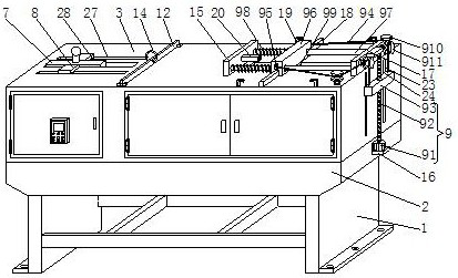
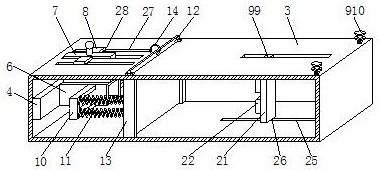
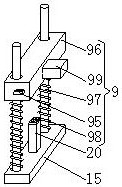
[0031]A high-precision detection device for semiconductor luminescence, comprising a support frame 1, a workbench 2 is bolted to the top of the support frame 1, a detection box 3 is bolted to the top of the workbench 2, and the left side of the front of the detection box 3 is passed through a joint. The first box door is hinged, and the front of the first box door is bolted with a con...


PUM


Abstract

The invention discloses a high-precision semiconductor luminescence detection device. The device comprises a supporting frame; the top of the supporting frame is in bolted connection with a workbench; the top of the workbench is in bolted connection with a detection box; the left side of the front surface of the detection box is hinged with a first box door through a hinge; the front surface of the first box door is in bolted connection with a control switch; and a moving mechanism is arranged at the top of the detection box. Through cooperation of a motor, a lead screw, a fixing plate, a fixing rope, a fixing ring, a connecting block and a positioning plate, a user can conveniently drive the fixing rope to move downwards through the motor, and through cooperation of a first guide wheel and a second guide wheel, the user can conveniently reverse the fixing rope; and therefore, the fixing rope can stably drive a moving plate and a brightness sensor to move rightwards through the positioning plate, the position of the brightness sensor can be changed, the brightness data is compared with standard brightness data at the same position, and the user can quickly know whether the semiconductor brightness is qualified or not.

Description

technical field [0001] The invention relates to the technical field of semiconductors, in particular to a high-precision detection device for semiconductor luminescence. Background technique [0002] Semiconductors are used in integrated circuits, consumer electronics, communication systems, photovoltaic power generation, lighting, high-power power conversion and other fields. For example, diodes are devices made of semiconductors. Whether from the perspective of technology or economic development, the importance of semiconductors The characteristics are very huge. Most of the electronic products, such as computers, mobile phones or digital recorders, have a very close relationship with the core units of semiconductors. Common semiconductor materials include silicon, germanium, gallium arsenide, etc., silicon It is the most influential one in the application of various semiconductor materials. [0003] Users often make semiconductors into luminous bodies. After the luminous...

Claims


Application Information

Patent Timeline
Patent Type & Authority Applications(China)
IPC IPC(8): G01J1/02G01J1/04
CPCG01J1/0271G01J1/0403
Inventor 庄小露
Owner 泗阳垠创运营管理有限公司
Why Eureka
Try Eureka