Check patentability & draft patents in minutes with Patsnap Eureka AI!

Connecting method of printed circuit board

A printed circuit board and connection method technology, which is applied in the structural connection of printed circuits, printed circuits, printed circuits, etc., can solve problems such as difficulty in ensuring the relative accuracy of wires and substrates, difficulty in accuracy, and reduction in the area of ​​mountable components

Inactive Publication Date: 2006-06-28
FUJITSU GENERAL LTD +1
View PDF1 Cites 0 Cited by
  • Summary
  • Abstract
  • Description
  • Claims
  • Application Information

AI Technical Summary

Problems solved by technology

[0014] 1. Since the formed wire must pass through the frame to make the wire and the frame integrally formed into a mold to make the terminal, the price of the terminal itself is high
[0015] 2. Since the upper end of the wire is to be inserted into the through hole of the control board, it is required to manage the relative position of the wire and the connection hole to a specified accuracy, and it is difficult to maintain the specified accuracy by molding alone
[0016] 3. Since the frame of the terminal block is a "mouth" shape, the area of ​​the terminal block on the substrate is large, resulting in a reduction in the area of ​​the actual mountable components
[0017] 4. Since the terminal material resin has a temperature limit, strict temperature management and engineering management must be carried out when welding the connection joint between the connection part and the substrate
[0018] That is to say, in the conventional connection structure, since the molded terminal is mounted on the substrate after forming, it is difficult to ensure the relative accuracy of the wire and the substrate.

Method used


Image

  • Connecting method of printed circuit board
  • Connecting method of printed circuit board
  • Connecting method of printed circuit board

Examples


Embodiment Construction

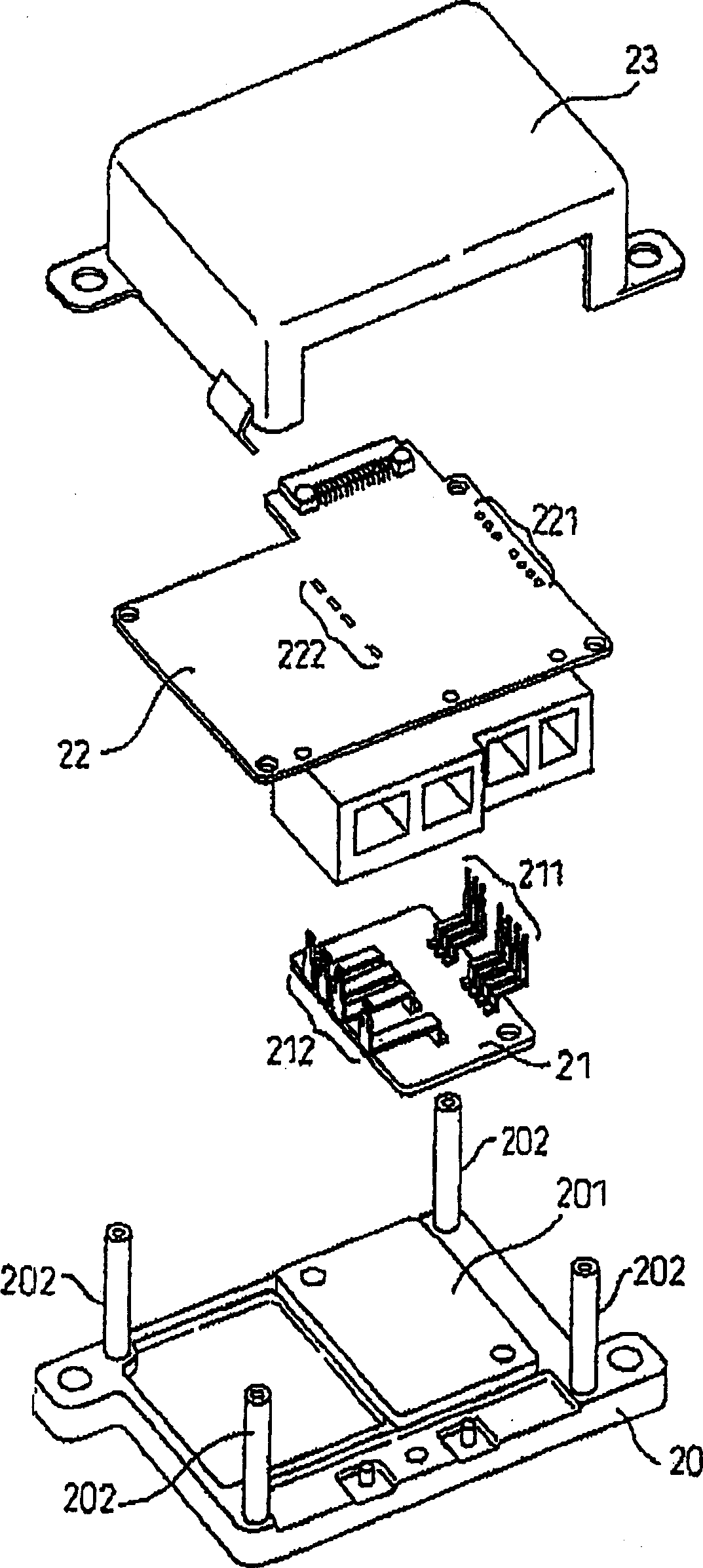
[0035] figure 2 It is a perspective view of the connection structure of the printed circuit board in the present invention, which is composed of a substrate 20 , a power substrate 21 , a control substrate 22 , and a cover 23 .

[0036] The base plate 20 is a cast product of aluminum, and the power board 21 , the control board 22 , and the cover 23 are fixed while radiating heat generated by the fastened power board.

[0037] In the power board 21, for example, the power control element of the IGBT is mounted, and at the same time, the crank-shaped control wire 211 and the power wire 212 are connected by soldering, but the control wire 211 and the power wire 212 are not the resin frame in the conventional structure. stand on the substrate 21 independently.

[0038] The method of attaching the control wire 211 and the power wire 212 to the power board 21 will be described later.

[0039] The power substrate 21 is tightly fixed on the base formed on the substrate by screws thr...


PUM


Abstract

By forming a terminal at a tip of a lead part of a lead frame, and by fixing this terminal and a connecting pad which was formed on an upper surface of a first printed circuit board, the lead frame is attached to the first printed circuit board. By cutting off a frame part and a tie bar part from the lead frame which was attached to the first printed circuit board, the lead part is separated, and forming is applied to the lead part so as for its tip to be extended over the first printed board. After the lead part which is expanded upward is inserted into a through-hole which was opened in a second printed circuit board, by soldering the lead part and the through-hole, the first printed circuit board and the second printed circuit board are electrically connected.

Description

technical field [0001] The invention relates to a connection structure and a connection method of printed circuit boards, in particular to a connection method of printed circuit boards with laminated configuration. Background technique [0002] In order to control the power supplied from the power source to the load, a control module is inserted into the power supply line. [0003] In this control module, in addition to a power control element for controlling electric power, a control element for controlling the power control element is generally mounted. [0004] Therefore, a common control module is composed of a control substrate for controlling elements and a power substrate on which power control elements are mounted, that is, two types of substrates. The electrical connections between the substrates are made using copper wires. [0005] Furthermore, lead wires are generally fixed at predetermined positions by resin frames (see Patent Document 1). [0006] Furthermor...

Claims


Application Information

Patent Timeline
Patent Type & Authority Patents(China)
IPC IPC(8): H05K1/02H05K1/11H05K1/14H01R43/02H05K3/34H05K3/36H05K7/14
CPCH05K7/142H01R43/0256H05K2201/10924H05K3/368H05K3/3447H05K3/3426H01R12/52H01R43/0263H05K2201/10757Y10T29/49151Y10T29/4913Y10T29/49135Y10T29/49149Y10T29/515Y10T29/53174Y10T29/49153Y10T29/53183Y10T29/5142Y10T29/49144Y10T29/49128Y10T29/53178Y10T29/49121Y10T29/49139Y10T29/49789
Inventor 太田隆山田一秋辻井清真锅秀一
Owner FUJITSU GENERAL LTD
Features
  • R&D
  • Intellectual Property
  • Life Sciences
  • Materials
  • Tech Scout
  • Unparalleled Data Quality
  • Higher Quality Content
  • 60% Fewer Hallucinations
Learn More