Color filtering device and fabricating method

A manufacturing method and a color filter layer technology, applied in optics, nonlinear optics, instruments, etc., can solve the problems of friction roller damage, alignment material layer damage, alignment material layer damage, etc.

Active Publication Date: 2007-02-21
AU OPTRONICS CORP
View PDF0 Cites 2 Cited by
  • Summary
  • Abstract
  • Description
  • Claims
  • Application Information

AI Technical Summary

Problems solved by technology

[0007] The purpose of the present invention is to provide a method for manufacturing a color filter substrate, which solves the problem that the alignment material layer is damaged due to the fact that the friction roller is easily damaged during the alignment rubbing process.
[0008] Another object of the present invention is to provide a color filter substrate, the peripheral area of ​​which has a special design to solve the problem of damage to the alignment material layer caused by the alignment rubbing process

Method used


Image

  • Color filtering device and fabricating method
  • Color filtering device and fabricating method
  • Color filtering device and fabricating method

Examples


no. 1 example

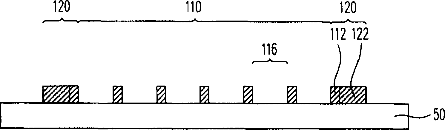
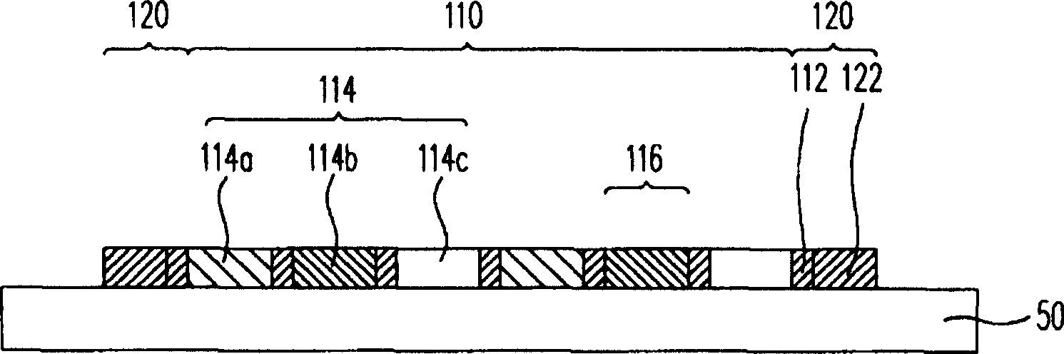
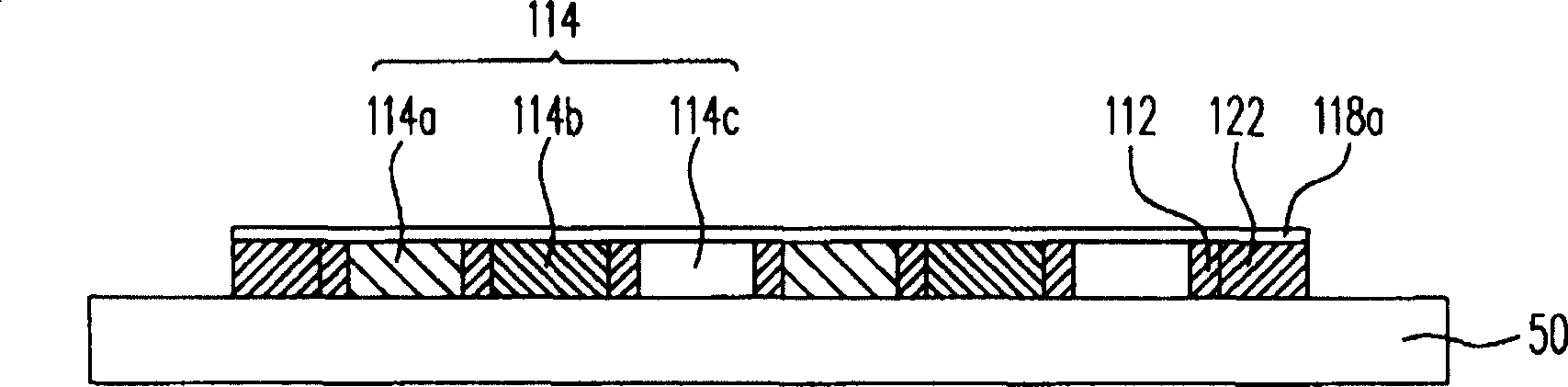
[0051] Figure 2A to Figure 2F It is a schematic cross-sectional view of a manufacturing method of a color filter substrate according to a preferred embodiment of the present invention. Please refer to Figure 2A Firstly, a transparent substrate 50 is provided, which has a display area 210 , a peripheral area 220 and a buffer area 230 , and the peripheral area 220 is located around the display area 210 . Next, a light-shielding pattern layer 212 is formed on the peripheral area 220 on the transparent substrate 50 . In one embodiment, the light-shielding pattern layer 212 is further formed in the display area 210, and the light-shielding pattern layer 212 formed in the display area will define a plurality of sub-pixel areas 216 in the display area 210 of the transparent substrate 50, thus The light-shielding pattern layer located in the display area is also called the light-shielding black matrix 226 . The light-shielding pattern layer 212 formed on the peripheral area 220 o...

no. 2 example

[0064] In addition to using the red filter pattern, green filter pattern or blue filter pattern as the material of the buffer pattern, the present invention can also use the same material as the light-shielding pattern layer as the material of the buffer pattern, but the design of the pattern is different from that of the buffer pattern. The first embodiment is different.

[0065] exist Figure 8A to Figure 8E Only the partial light-shielding frame 222 located in the peripheral area and the buffer patterns 224a, 224b, 224c, 224d, 224e located in the buffer zone are shown. And other film layers such as the color filter layer, light-shielding pattern layer, electrode layer, alignment material layer in the display area are the same as the above-mentioned first embodiment (such as image 3 shown), so it will not be repeated here.

[0066] Please refer to Figure 8A , in this embodiment, the buffer pattern is composed of a plurality of patterns 224a arranged on the edge of the l...

no. 3 example

[0071] The cushioning pattern of the present invention can utilize transparent resin (that is, the material of the spacer) as a cushioning in addition to the red filter pattern, the green filter pattern, the blue filter pattern, and the light-shielding pattern layer as the buffering pattern material. The texture of the pattern. In particular, in this embodiment, the buffer pattern is composed of a plurality of patterns, and the arrangement density of these patterns gradually decreases from the light-shielding pattern layer to the place away from the light-shielding pattern layer.

[0072] exist Figure 9A to Figure 9C Only the partial light-shielding frame 222 located in the peripheral area and the buffer patterns 224f, 224g, 224g' located in the buffer zone are shown in FIG. And other film layers such as the color filter layer, light-shielding pattern layer, electrode layer, alignment material layer in the display area are the same as the above-mentioned first embodiment (such...


PUM


Abstract

A method for preparing color filtering device includes providing a transparent base plate, forming a light shading pattern layer around peripheral region and in display region of transparent base plate and forming a color filtering layer is said display region, forming a buffer pattern in buffer region and forming an orientated material layer covering partial color filtering layer and partial light shading pattern layer as well as partial buffer pattern then carrying out an orientated friction process on orientated material layer starting from position of buffer pattern.

Description

technical field [0001] The present invention relates to a color filter substrate and a manufacturing method thereof, and in particular to a color filter substrate capable of avoiding defects in an alignment material layer due to a rubbing process and a manufacturing method thereof. Background technique [0002] With the high development of computer performance, Internet and multimedia technology efficiency, image information has gradually changed from analog information to digital information. In order to adapt to the modern life style, the weight and size of many electronic devices have also become lighter and thinner. Taking the display device as an example, it has changed from a cathode ray tube (Cathode Ray Tube, CRT) with large size, high radiation, heavy weight and high energy consumption to a thin, light weight, flat screen. Display devices with features such as , no radiation, and low energy consumption are the mainstream. For example, liquid crystal display (Liqui...

Claims


Application Information

Patent Timeline
Patent Type & Authority Applications(China)
IPC IPC(8): G02F1/1335
Inventor 赖纪光李如玉吕安序许淑卿张禄坤
Owner AU OPTRONICS CORP
Why Eureka
Try Eureka