

Power network design method based on power consumption distribution
A power network and design method technology, applied in computing, electrical digital data processing, instruments, etc., can solve problems such as aggravating the shortage of wiring resources, and achieve the effect of saving software computing time and facilitating changes
- Summary
- Abstract
- Description
- Claims
- Application Information
AI Technical Summary
Problems solved by technology
Method used
Image


Examples
Embodiment Construction
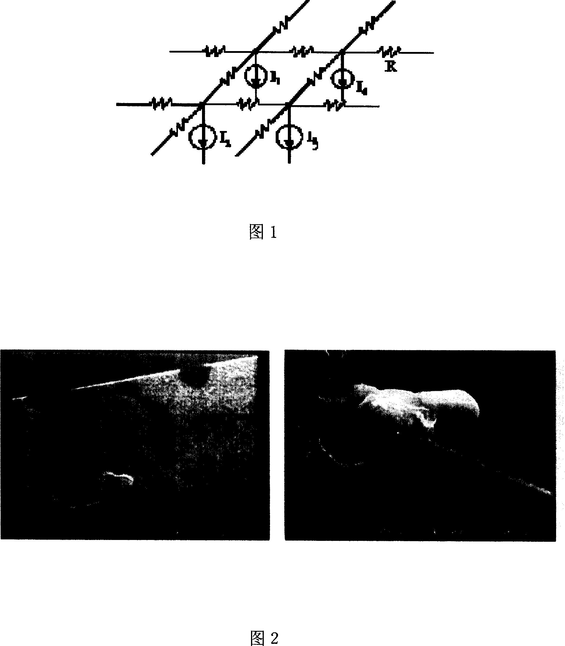
[0029] Figure 1 is a schematic diagram of the power grid IR-drop, each power grid line can be equivalent to an impedance.
[0030] Voids and hillocks caused by migration in Figure 2, the current causes metal ions to migrate to form voids and hillocks.
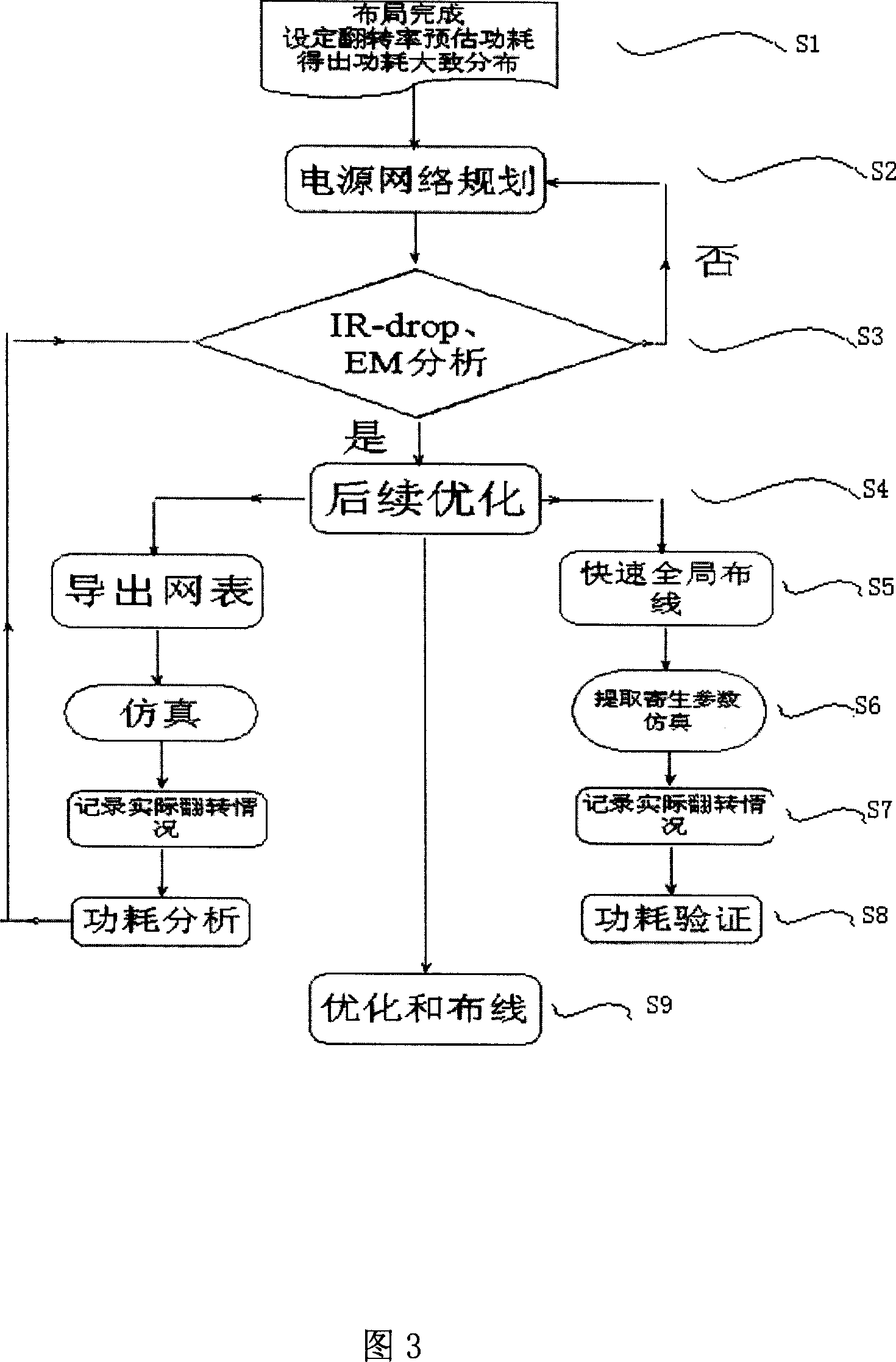
[0031] The detailed process of power network planning based on power consumption distribution in Figure 3, the specific steps are as follows:
[0032] Step S1, after the layout is completed, set a reasonable flip rate to estimate the power consumption;
[0033] Step S2, use the estimated power consumption value to guide the power network planning, determine the approximate metal layer of the network, and estimate the line width and spacing required for each layer according to the metal electrical parameters of each layer;
[0034] Step S3, conduct IR-drop and EM analysis based on the preliminary power network, and determine whether the planning needs to be changed;
[0035] Step S4, perform subsequent optimization after modif...
PUM
 Abstract
Description
Claims
Application Information