Multi-function chipset and related method

a multi-functional chip and chip technology, applied in the direction of instruments, electric digital data processing, etc., can solve the problems that the time and cost involved in the semiconductor procedure of the two chipsets cannot be reduced, and achieve the effect of reducing the time and cost of producing the chips

Inactive Publication Date: 2006-05-04
VIA TECH INC
View PDF12 Cites 5 Cited by
  • Summary
  • Abstract
  • Description
  • Claims
  • Application Information

AI Technical Summary

Benefits of technology

[0009] As known by those skilled in the art, the clock frequency of each input/output signal of the input/output pad is one of the most important design considerations. Designers have to think about the clock frequency of the input/output signals, and then the designers can determine the spacing between two input/output pads, wire and layout configuration according to the above-mentioned clock frequency in order to prevent noises between input/output pads (for example, cross-talk or clock skew and jitter). In the present invention, the similar clock frequencies of the AGP and PCI-X buses are well utilized so that the two bus controllers can be integrated in the same IC and share the same layout of input/output pads. In a preferred embodiment of the present invention, a multiplexer module having at least one multiplexer is utilized to control electrical connections between the two bus controllers and

Problems solved by technology

Furthermore, time and cost involved in the semiconductor procedure of the two chipsets can n

Method used


Image

  • Multi-function chipset and related method
  • Multi-function chipset and related method
  • Multi-function chipset and related method

Examples


Embodiment Construction

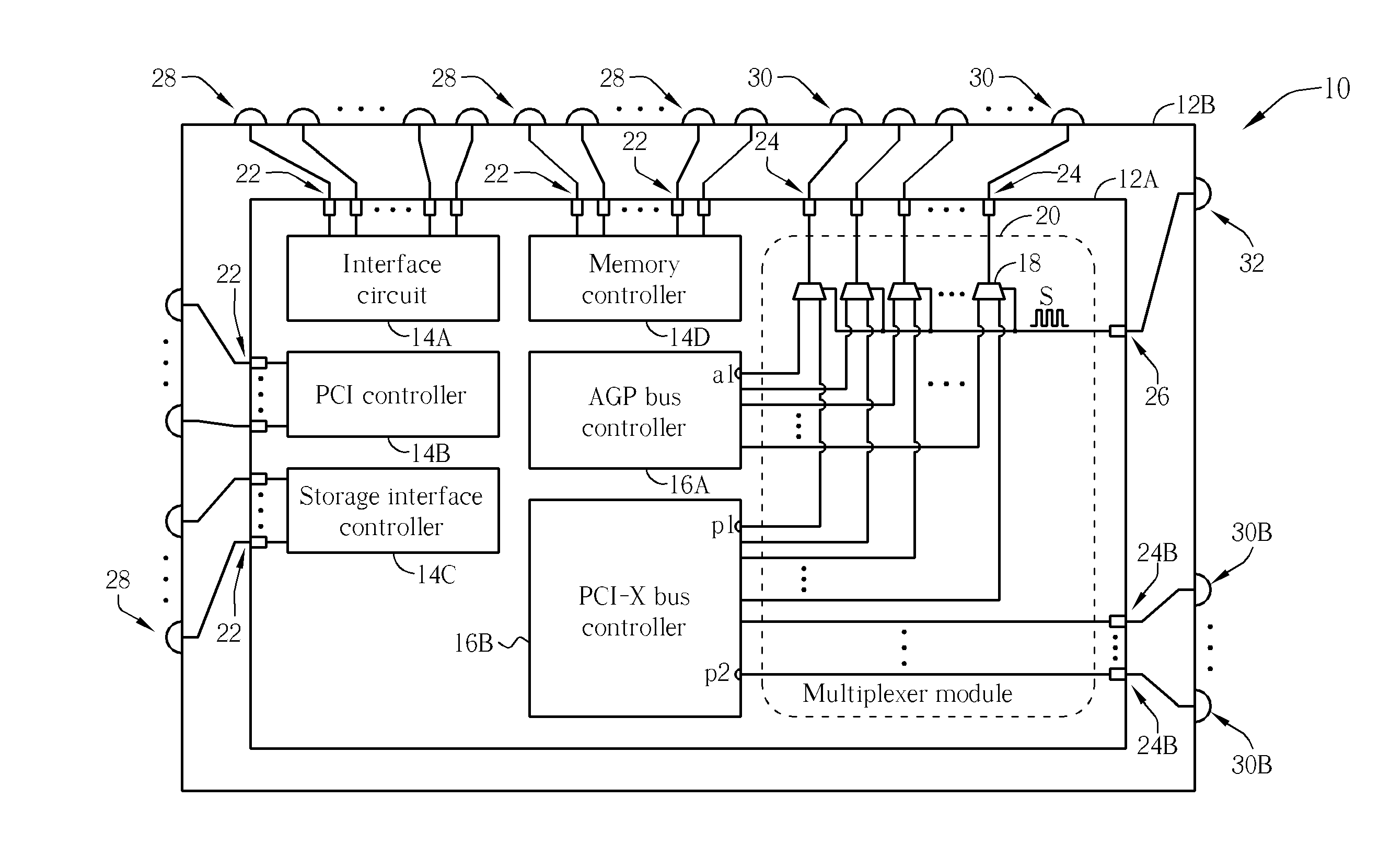
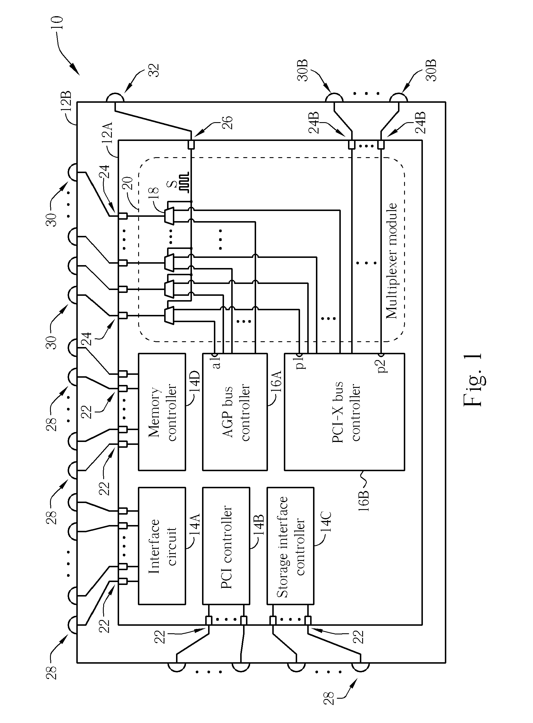
[0016] Please refer to FIG. 1, which is a diagram of a chipset 10 of an embodiment according to the present invention. The chipset 10 has an IC 12A with a packaging substrate 12B. The IC 12A comprises a peripheral component interconnect (PCI) controller for managing PCI buses, a storage interface controller 14C for controlling storage devices (for example, the hard disk or optical disk), a memory controller 14D for accessing memory, and an interface circuit 14A for managing the chipset 10 and the data exchange between the chipset 10 and the CPU. In addition, the IC 12A can selectively comprise an audio circuit for managing audio outputs, a display processing circuit for managing graphic signals, or a network controller. The above-mentioned circuits can receive / transfer signals or biases through the input / output pads 22 of the IC 12A. When the IC 12A is packaged on the packaging substrate 12B, the input / output pads 22 can be electrically connected to each corresponding ball (pin) 28 ...


PUM


Abstract

Multi-function chipset and related design/manufacturing method for realizing different kinds of chipsets respectively supporting accelerated graphic port (AGP) bus and peripheral component interconnect extended (PCI-X) bus. The integrated circuit of the chipset includes both the AGP and PCI-X bus controllers, which share a common I/O pad configuration, and the chipset is selected to be an AGP-supported chipset or a PCI-X supported chipset by pin strapping. Also, the chipset can be packaged with different wire bonding configurations to alternatively realize chipsets supporting AGP bus or PCI-X bus.

Description

BACKGROUND OF INVENTION [0001] 1. Field of the Invention [0002] The invention relates to a multi-function chip set and related design / manufacturing method, and more particularly, to a chip set and related design / manufacturing method capable of utilizing a single IC to implement chipsets with different functions. [0003] 2. Description of the Prior Art [0004] Computer systems are the most important hardware foundation in today's modern information society. As the need for computer systems increases, demands of different users of the computer systems have become more apparent. In order to meet these demands, the information service provider discloses different related components of computer systems. As known by those skilled in the art, the computer system utilizes chipsets to manage / control data exchanges among the CPU, system memory, graphic acceleration cards, other cards / circuits, and peripheral devices. For example, the chip set is electrically connected to the graphic acceleratio...

Claims


Application Information

Patent Timeline
IPC IPC(8): G06F13/00
CPCG06F13/4027
Inventor LIN, CHI-HSINGYU, CHIA-HSING
Owner VIA TECH INC
Why Eureka
Try Eureka