Two-dimensional image detector

a detector and two-dimensional technology, applied in the field of two-dimensional image detectors, can solve the problems of difficulty in carrying and preserving, disadvantages in assembling, and the life duration of the ic elements provided on the back surface of the base board, and achieve the effects of reducing weight and the size of the sensor section, reducing the strength required for the sensor section, and improving the handling of the sensor section

Inactive Publication Date: 2006-08-03
SHIMADZU CORP
View PDF1 Cites 7 Cited by
  • Summary
  • Abstract
  • Description
  • Claims
  • Application Information

AI Technical Summary

Benefits of technology

[0011] According to a first aspect of the present invention, a base board, which loads an electronic component such as a signal processing circuit and a power supply circuit thereon, is separated from a sensor section having an active matrix substrate, and disposed on a case side. Further, the case has a mechanical strength enough to support the active matrix substrate without deformation of the active matrix substrate.
[0012] With the above-mentioned structure, the strength required for the sensor section can be minimized, which enables the weight and the size of the sensor section to be reduced. As a result, the handling of the sensor section can be improved.
[0016] Therefore, as mentioned in the first aspect of the present invention, the above described structure in the third aspect of the present invention also improves the handling of the sensor section since the weight of the sensor section can be reduced.
[0019] According to a fifth aspect of the present invention, the reinforcing board is integrated with the active matrix substrate so as to reinforce the strength of the active matrix substrate.

Problems solved by technology

However, the above explained structure of related-art two-dimensional image detector has a problem of the life duration of the IC elements provided on the back surface of the base board 5 being shortened, disadvantage in assembling and difficulty in carrying and preserving (hereinafter referred to as handling) the active matrix substrate 2 especially when the active matrix substrate is a large type.
Although some adjunctive tools and jigs are used because of such a complex assembling work, workability of which is bad in that it results in increasing of working time due to the strain from a careful operation not to hurt oneself or not to damage the components by error during the operation.
In addition, the sensor section S having precision components has a difficulty in handling due to its several ten kilograms of weight and a carefulness required when carrying and preserving without a cover.

Method used


Image

  • Two-dimensional image detector
  • Two-dimensional image detector
  • Two-dimensional image detector

Examples


Embodiment Construction

[0024] Preferred embodiments of the present invention will be explained below.

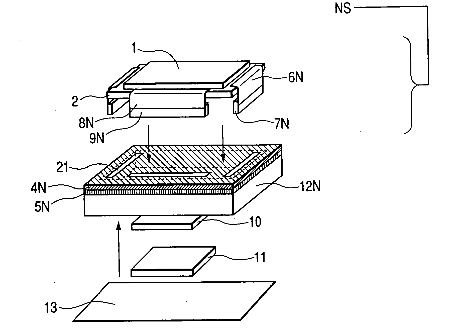
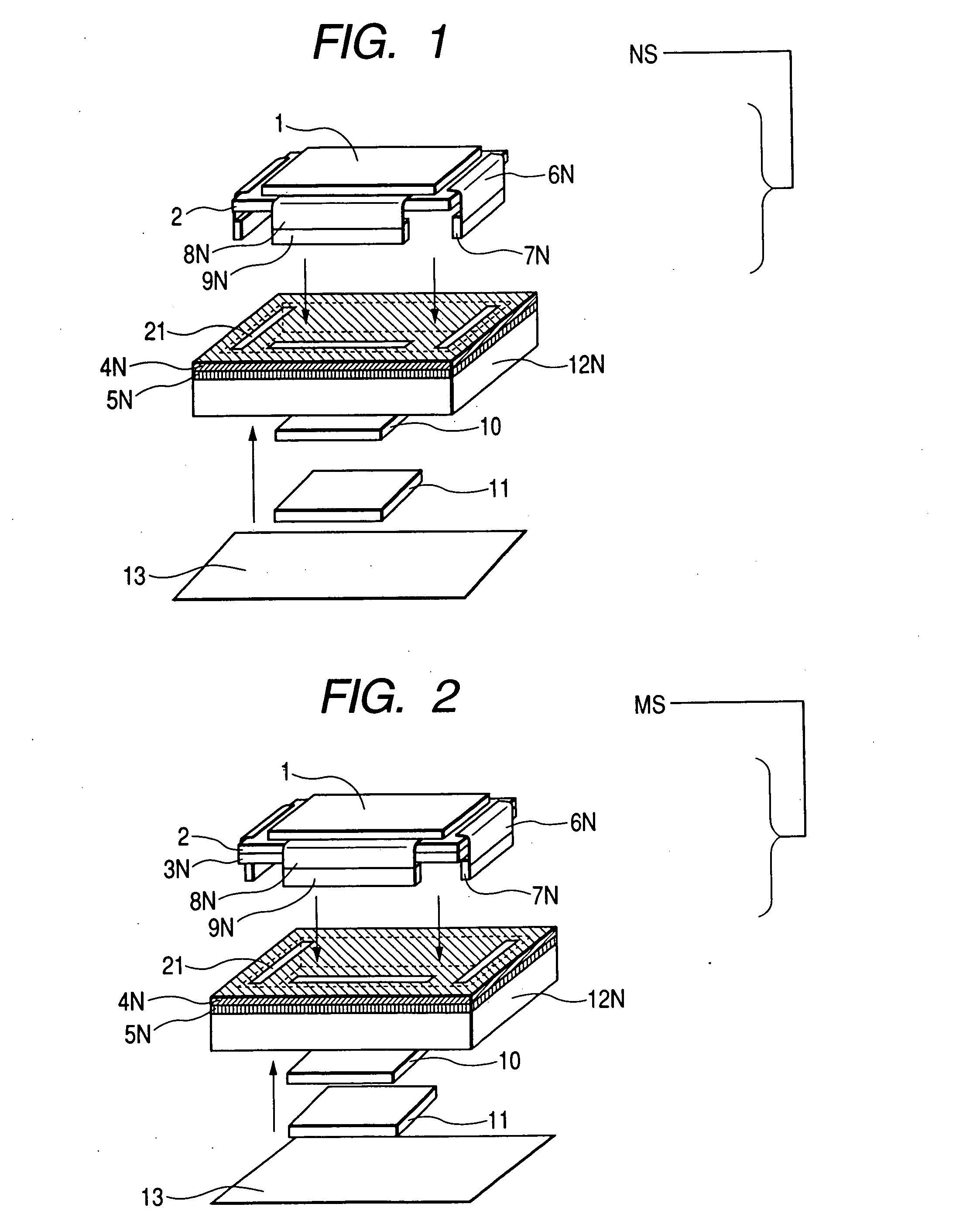
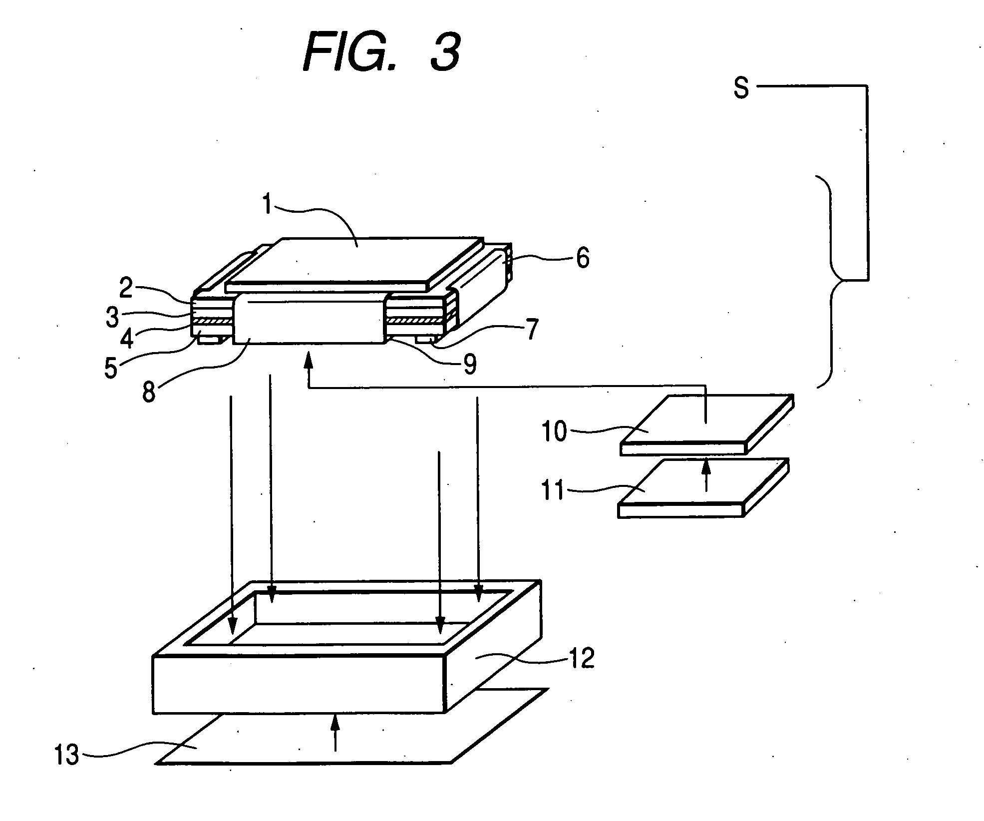
[0025] A Pb plate and a base board loading an electronic component such as a signal processing circuit and a power supply circuit are disposed on a case, and the case has a mechanical strength enough to support the active matrix substrate without deformation or destruction of the active matrix substrate. Further, slits are provided at the Pb plate and the base board. A small-signal amplifier control substrate is inserted inside the case through the slits without bending a small-signal amplifier, and connected to a coupling component such as a socket or connector, which conforms to the shape of the end portion of the small-signal amplifier control substrate, so that the active matrix substrate and a circuit provided on the back surface of the board are detachably electrically connected to each other.

[0026]FIG. 1 is a view showing the structure of a two-dimensional image detector of an embodiment according...


PUM


Abstract

A Pb plate and a base board loading electronic components such as a signal processing circuit and a power supply circuit are disposed on a case side so as to decrease the weight and the thickness of a sensor section. Besides, the case has a mechanical strength enough to support the active matrix substrate without deformation. Further, a small-signal amplifier control substrate and a gate driver control circuit substrate are inserted inside the case through slits and electrically connected to the electronic components loaded on the base board.

Description

[0001] The present invention claims foreign priority to Japanese patent application no. 2005-027740, filed on Feb. 3, 2005, the content of which is incorporated herein by reference. BACKGROUND OF THE INVENTION [0002] 1. Field of the Invention [0003] The present invention relates to a two-dimensional image detector which detects a two-dimensional distribution of radial or electromagnetic rays such as particle rays, x-rays, visible light, infrared light, etc., (hereinafter referred as radial rays) as an image, and is used for a medical radial imaging apparatus, an industrial nondestructive inspection apparatus etc. [0004] 2. Description of the Related Art [0005] In a two dimensional image detector, an active matrix substrate is integrated with an image sensor for converting radial rays to electric charge signals and a base board. The base board loads an electronic circuit including IC elements such as a small-signal amplifier for the electric charge signals, a control circuit, a gate ...

Claims


Application Information

Patent Timeline
Patent Type & Authority Applications(United States)
IPC IPC(8): H01L27/00G01J1/02G01T1/20G01T1/24G01T7/00H01L27/14H04N5/32H04N5/335H04N5/374
CPCH01L27/14618H01L27/14623H01L27/14683H01L2924/0002H01L2924/00
Inventor YOSHIMUTA, TOSHINORI
Owner SHIMADZU CORP
Why Eureka
Try Eureka