

Design structure to eliminate step response power supply perturbation
a step response and design structure technology, applied in the direction of electronic switching, pulse technique, instruments, etc., can solve the problems of step response, voltage gradient, step response remains a serious problem, and the voltage at the operating circuit is reduced relativ
- Summary
- Abstract
- Description
- Claims
- Application Information
AI Technical Summary
Benefits of technology
Problems solved by technology
Method used
Image

Examples
Embodiment Construction
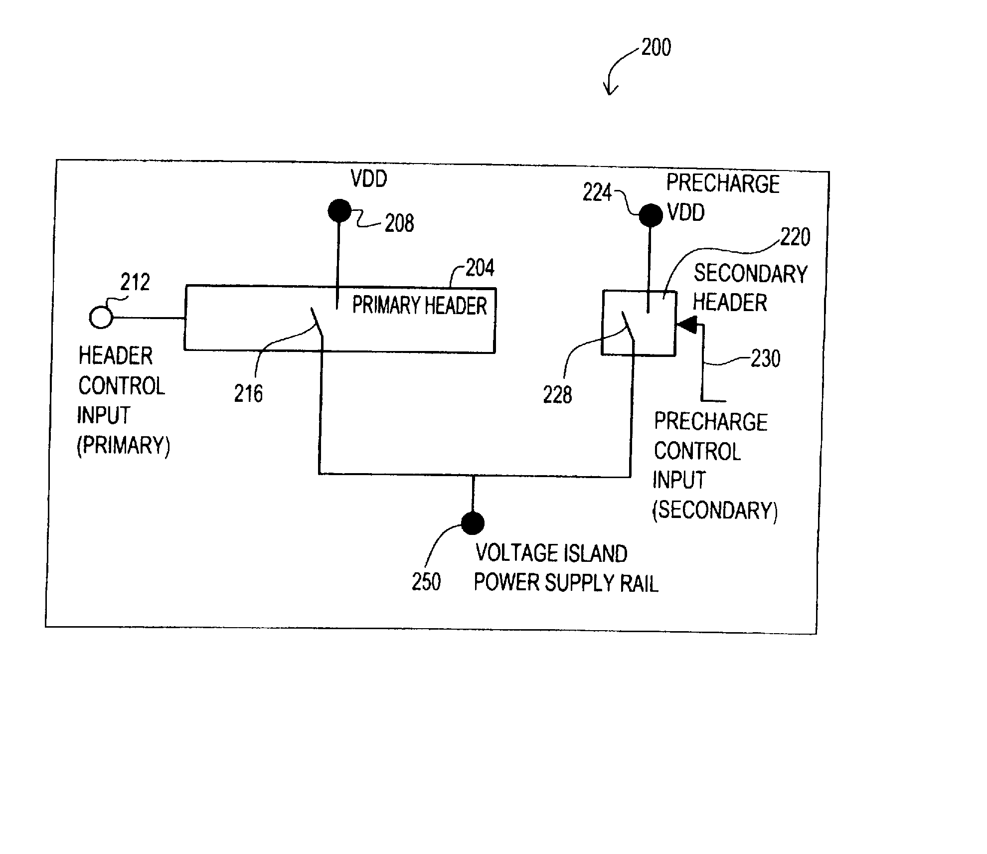
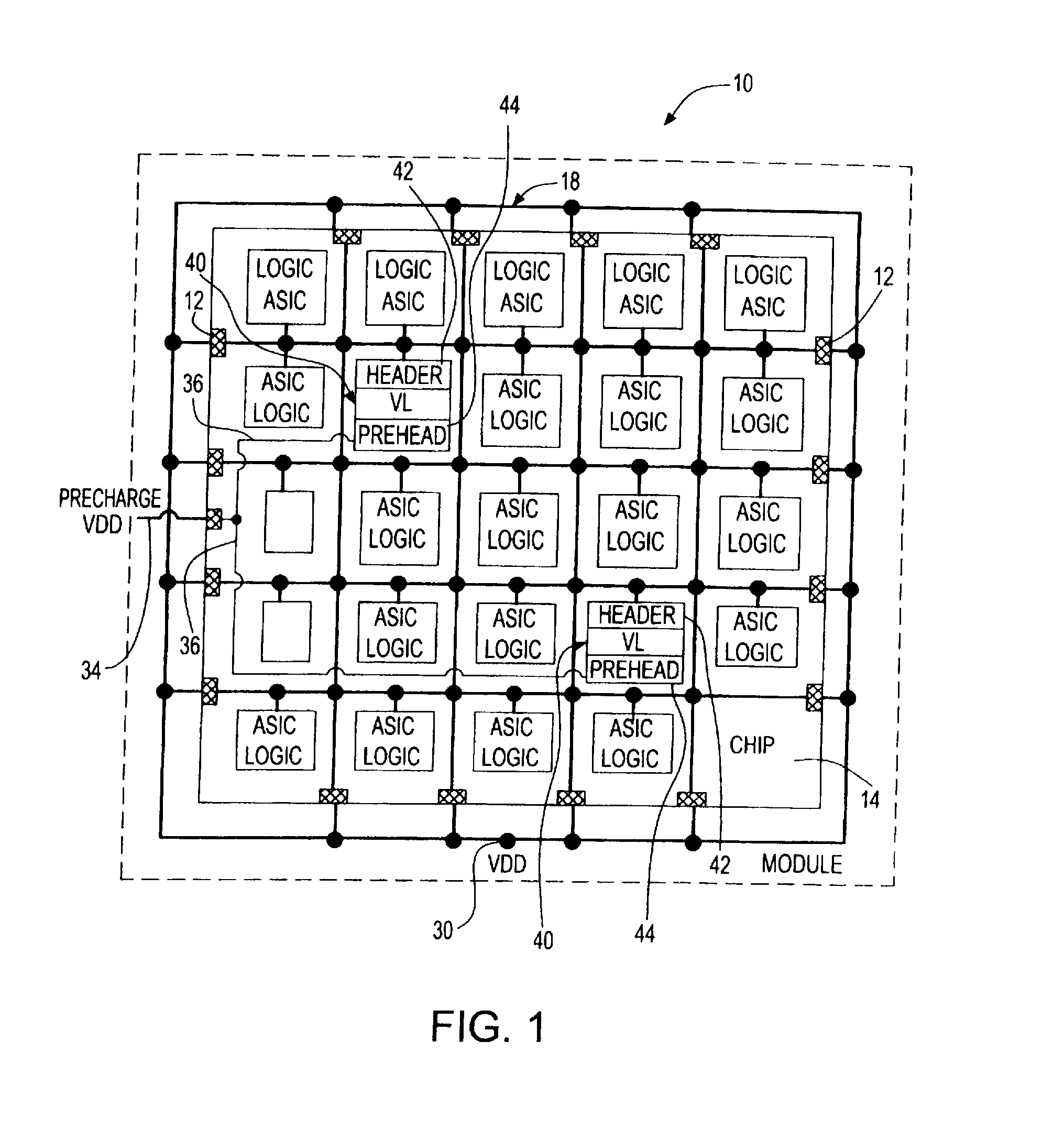
[0041] The present invention provides a design structure of a new header design and image / package bus plan which eliminates the voltage island power-up issue of a step response during power up (di / dt) resulting in power supply perturbation. In addition, the present invention results in both efficient management of voltage island power state transition and efficient central management of voltage island power up. Further, the present invention teaches a topology for mitigation of island power-off (di / dt) transient mitigation.
[0042] The present invention provides a power on design structure for an IC voltage island having primary and secondary header circuits where the secondary header circuit is enabled and the island is pre-charged / repowered in a static mode. Then, the secondary header is disabled and the primary header is enabled to provide connectivity to a power bus with functional current-load capability. Finally, the island data / clock boundaries are enabled to start IC function...
PUM
 Abstract
Description
Claims
Application Information