Electronic device and method of manufacturing the same

a technology of electronic devices and manufacturing methods, applied in thermoelectric devices, discharge tubes/lamp details, discharge tubes luminescent screens, etc., can solve the problem of no convenient method of direct patterning of insulating materials such as fluorinated organic polymers

Active Publication Date: 2008-06-19
SAMSUNG DISPLAY CO LTD
View PDF10 Cites 24 Cited by
  • Summary
  • Abstract
  • Description
  • Claims
  • Application Information

AI Technical Summary

Benefits of technology

[0007]Some embodiments described herein provide a method of manufacturing an electronic device including a bank structure requiring a fewer number of processes in which a direct patterning of insulating layers, such as fluorinated organic polymers, is possible by using cost-efficient techniques, such as inkjet printing, As well as an electronic device manufactured using the method.

Problems solved by technology

According to the present state of the art, there is no convenient method of direct patterning insulating materials such as fluorinated organic polymers.
However, due to ink wetting issues, a bank structure is used in many inkjet patterning processes to provide the desired pattern, for example, to reduce ink overflow into adjacent pixel areas of the OLED display device.

Method used


Image

  • Electronic device and method of manufacturing the same
  • Electronic device and method of manufacturing the same
  • Electronic device and method of manufacturing the same

Examples


Embodiment Construction

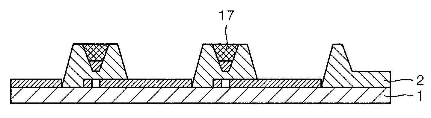
[0049]Hereinafter, certain embodiments will now be described more fully with reference to the accompanying drawings, which illustrate exemplary embodiments. In general, it shall be noted that reference characters are not attached to every element in every drawing for clarity, but only when an element is shown the first time. Therefore, it should be understood that elements having the same hatching represent the same functional elements.

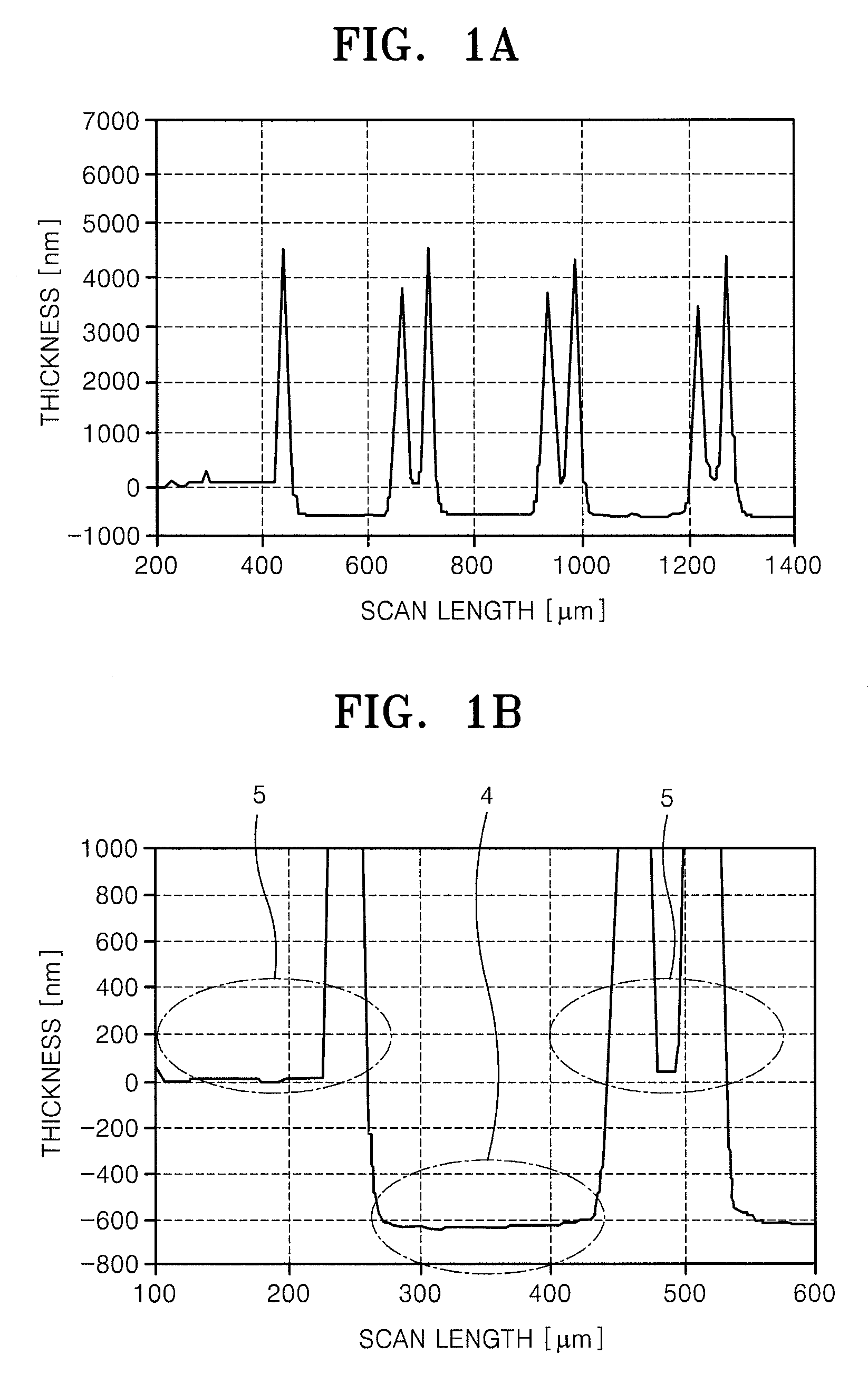
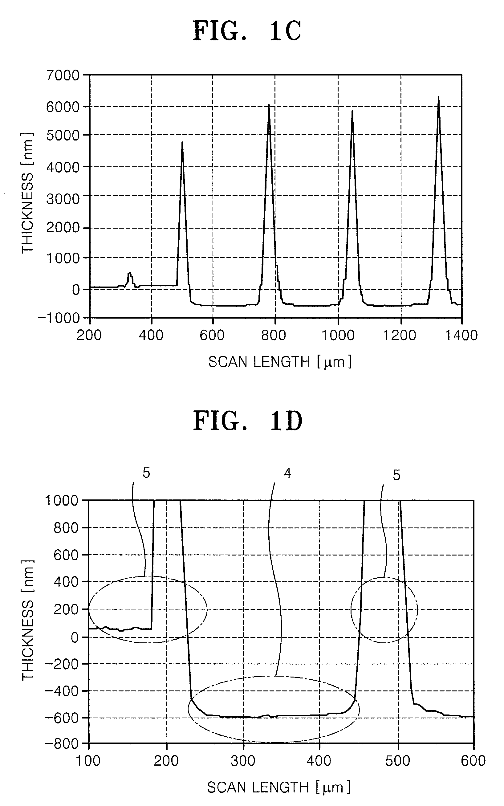
[0050]FIGS. 1A to 1D are cross-sectional views an embodiment of a bank structure on a substrate employed in the manufacture of an organic light emitting diode (OLED). The units of the horizontal axes are μm and the units of the vertical axes are μm in FIGS. 1A-1D.

[0051]FIG. 1A shows a cross-sectional view an embodiment of the bank structure of the substrate that can be used for the manufacture of an OLED. FIG. 1B shows an enlarged view of the bank structure of the substrate of FIG. 1A. In order to obtain a substrate having the bank structure that can ...


PUM


Abstract

Provided are an electronic device including a bank structure and a method of manufacturing the same. The method of manufacturing the electronic device requires a fewer number of processes and comprises a direct patterning of insulating layers, such as fluorinated organic polymer layers, is possible using cost-efficient techniques such as inkjet printing.

Description

CROSS REFERENCE TO RELATED APPLICATIONS[0001]This application claims the benefit of European Patent Application No. 06 126 004.8, filed on Dec. 13, 2006 and Korean Patent Application No. 10-2007-0036180, filed Apr. 12, 2007, the disclosures of which are incorporated by reference in their entireties.BACKGROUND[0002]1. Technical Field[0003]This disclosure relates generally to an electronic device and a method of manufacturing the same, and more particularly, to an organic light emitting diode comprising a bank structure and a method of manufacturing the same; and also relates to an electronic device comprising a bank structure having conductive lines and a method of insulating the conductive lines used in the electronic device; and further relates to a method of forming a gate electrode of a thin film transistor (TFT) of an organic light emitting diode (OLED) and an electrophoretic device.[0004]2. Description of the Related Art[0005]According to the present state of the art, there is ...

Claims


Application Information

Patent Timeline
Patent Type & Authority Applications(United States)
IPC IPC(8): H01L51/00H01L21/02H01L51/40
CPCH01L27/3295H01L51/0004H01L51/0019H01L2924/0002H01L2924/00H10K59/122H10K71/13H10K71/236
Inventor MATHEA, ARTHURFISCHER, JOERGSCHAEDIG, MARCUS
Owner SAMSUNG DISPLAY CO LTD
Why Eureka
Try Eureka