Optical waveguide mounted substrate and method of producing the same

a technology of optical waveguides and substrates, applied in the direction of instruments, cladded optical fibres, optical elements, etc., can solve the problems of working efficiency and production costs, and achieve the effects of facilitating the formation of reflecting mirrors for optical transmission, reducing production costs, and simplifying the structure of optical waveguides

Active Publication Date: 2009-03-19
SHINKO ELECTRIC IND CO LTD
View PDF7 Cites 15 Cited by
  • Summary
  • Abstract
  • Description
  • Claims
  • Application Information

AI Technical Summary

Benefits of technology

[0045]According to the exemplary embodiments of invention, as means for optical transmission, a reflecting mirror (for example, 45-degree inclined reflecting mirror) is formed on an electrical circuit substrate in extension of the production of the electrical circuit substrate. Therefore, the necessity for disposing the reflecting mirror structure in an optical waveguide is eliminated and the formation of the reflecting mirror for optical transmission is facilitated and the structure of the optical waveguide is simplified. According to the configuration, the optical waveguide can be formed on the electrical circuit substrate as extension of the production of the electrical circuit substrate. In the optical waveguide mounted substrate, the electrical circuit substrate and the optical waveguide, which are separately produced in the related art, can be collectively produced in extension of the production of the electrical circuit substrate. The number of man-hours and the production cost can be reduced.

Problems solved by technology

Therefore, the processes of producing the electrical circuit substrate, producing the optical waveguide (mirror component), and mounting the optical waveguide on the electrical circuit substrate must be separately conducted, thereby causing problems of the working efficiency and the production cost.
However, in this case, the structure of the 45-degree inclined reflecting mirror and the production process cause bottlenecks.

Method used


Image

  • Optical waveguide mounted substrate and method of producing the same
  • Optical waveguide mounted substrate and method of producing the same
  • Optical waveguide mounted substrate and method of producing the same

Examples


Embodiment Construction

[0053]Hereinafter, embodiments of the invention will be described in detail with reference to the accompanying drawings.

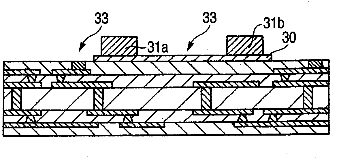
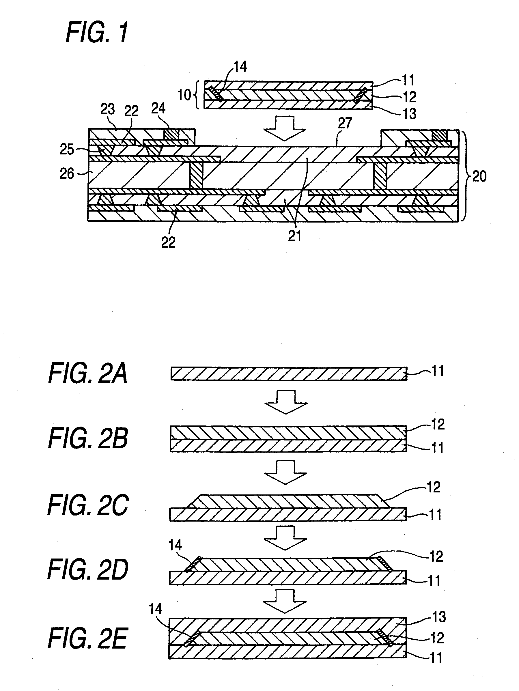
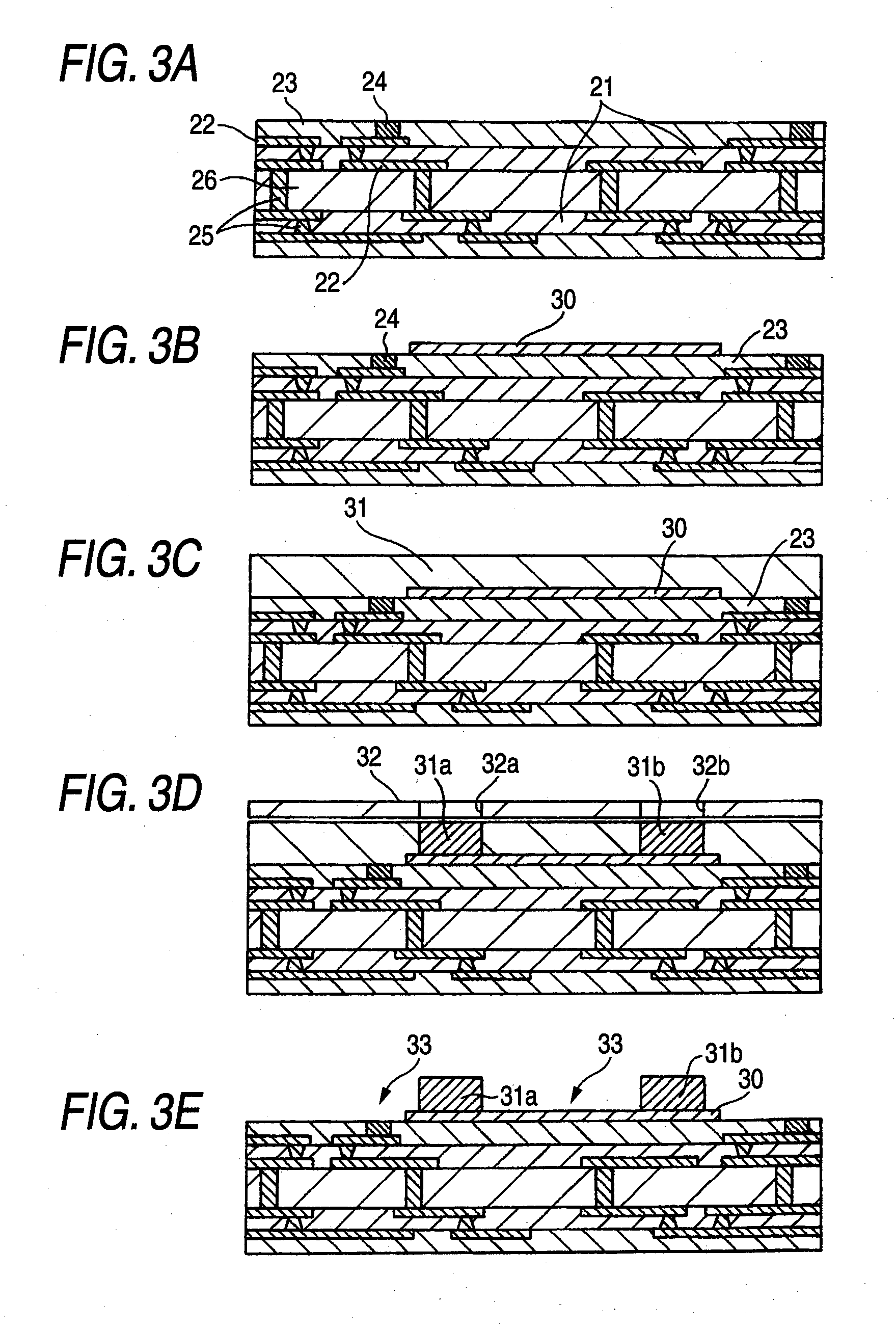
[0054]FIGS. 3 and 4 show sequential steps of a method of producing an optical waveguide mounted substrate of an embodiment of the invention. FIG. 3A is a section view of a multilayer electrical circuit substrate. The electrical circuit substrate shown in FIG. 3A comprises an insulating resin layer 21, a circuit pattern 22 made of Cu, a solder resist 23, a solder land 24, a via 25 connecting the circuit patterns (or a through-hole via), and an insulating core substrate 26 made of a material such as FR-4.

[0055]The surface of the electrical circuit substrate on which an optical waveguide is to be formed is configured by a face of the flat solder resist 23. The face of the solder resist 23 has an area required for forming a predetermined optical waveguide.

[0056]First, a lower cladding layer 30 of the optical waveguide is stacked on the face of the solder resist 23 as s...


PUM

PropertyMeasurementUnit
angleaaaaaaaaaa
angleaaaaaaaaaa
thicknessaaaaaaaaaa

Abstract

A lower cladding layer is formed on a surface of an electrical circuit substrate. A UV curable resin layer is stacked on the lower cladding layer. The resin layer is partly cured, and the other uncured resin layer is removed, thereby forming resin projections. The resin projections are processed so as to have an inclined face. Metal reflecting layers are formed on the inclined faces. A core layer is stacked on the lower cladding layer and the metal reflecting layers, and an upper cladding layer is stacked on the core layer.

Description

TECHNICAL FIELD[0001]The present disclosure relates to an optical waveguide mounted substrate which is used in photoelectric conversion of signal transmission, such as an opto-electric package or an opto-electric substrate, and a method of producing such an optical waveguide mounted substrate.RELATED ART[0002]As an optical communication device, a laser emitting device (VCSEL) is mainly used. In the case where such a device and a light receiving device (PD) are flip-chip mounted on a substrate or the like, light is perpendicularly emitted from the device toward the surface of the substrate.[0003]Therefore, a method is employed in which light is reflected at 90 degrees by an inclined mirror so that the light emission direction is parallel to the substrate plane.[0004]In related-art production of an opto-electric composite substrate, an electric substrate and an optical waveguide are separately produced, and these components are then combined with each other. The inclined mirror is pre...

Claims


Application Information

Patent Timeline
Patent Type & Authority Applications(United States)
IPC IPC(8): G02B6/12H01L21/02G02B6/02
CPCG02B6/4214G02B2006/1219H05K2201/2054H05K2201/09909H05K1/0274G02B6/12G02B6/13
Inventor YANAGISAWA, KENJI
Owner SHINKO ELECTRIC IND CO LTD
Why Eureka
Try Eureka