Display device with parallel data distribution

a display device and data technology, applied in the direction of electric variable regulation, process and machine control, instruments, etc., can solve the problems of large size of thin film transistors (tfts) made from amorphous or polycrystalline silicon, lower performance compared to conventional transistors made in crystalline silicon wafers, and non-uniform electrical performance and visual appearance of displays using such materials, so as to reduce the cost of driver circuitry and display manufacturing, reduce the complexity of wiring of display devices, reduce the effect of o

Active Publication Date: 2010-12-09
GLOBAL OLED TECH
View PDF11 Cites 48 Cited by
  • Summary
  • Abstract
  • Description
  • Claims
  • Application Information

AI Technical Summary

Benefits of technology

[0020]An advantage of the present invention is that the use of the selection circuit responsive to the pixel information is a more efficient design that reduces wiring complexity of the display device. Furthermore, a display device of the present invention is more tolerant of wiring and interconnection fa

Problems solved by technology

Thin-film transistors (TFTs) made from amorphous or polycrystalline silicon are relatively large and have lower performance compared to conventional transistors made in crystalline silicon wafers.
Moreover, such thin-film devices typically exhibit local or large-area non-uniformity across the glass substrate that results in non-uniformity in the electrical performance and visual appearance of displays employing such materials.
This technique is used because other schemes such as direct addressing (for example as used in memory devices) require the use of address decoding circuitry that is very difficult to form on a conventional thin-film active-matrix back plane, and is impossible to form on a passive-matrix back-plane as such a back-plane lacks trans

Method used


Image

  • Display device with parallel data distribution
  • Display device with parallel data distribution
  • Display device with parallel data distribution

Examples


Embodiment Construction

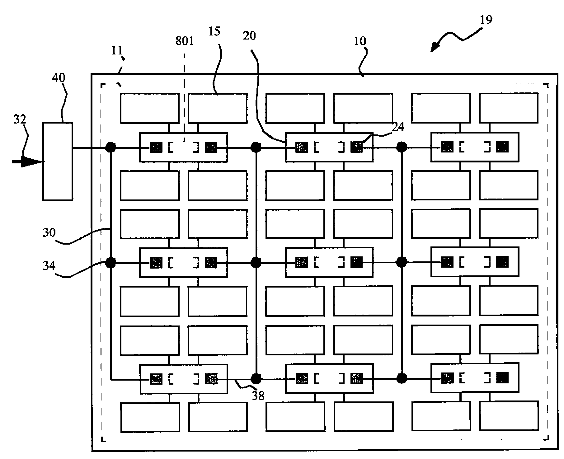
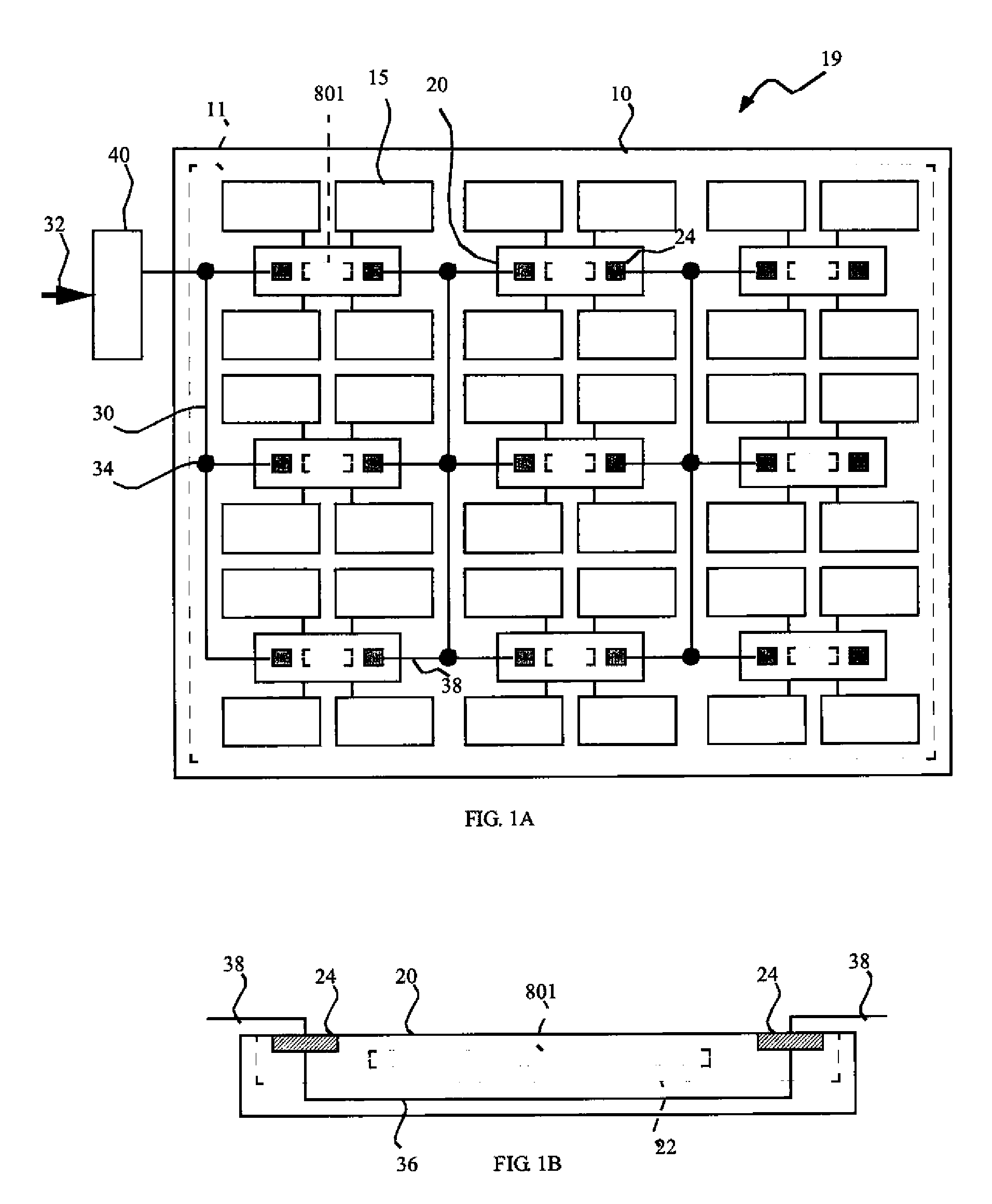
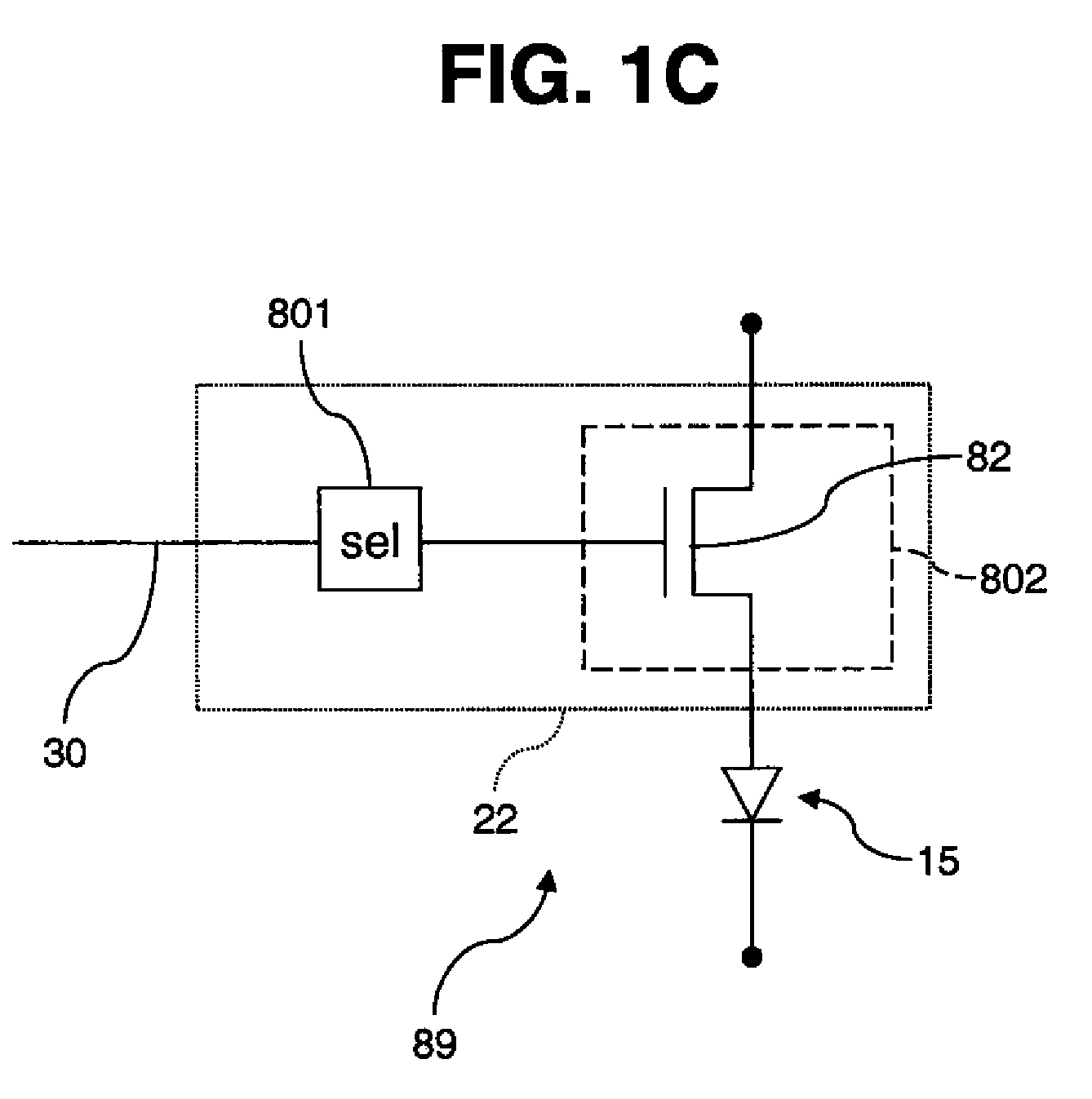
[0038]Referring to FIG. 10, a display device 19 responsive to a controller 40 includes a plurality of pixels 89, each having an optical element 15 and a driving circuit 802 for controlling the optical element 15 in response to selected pixel information. The pixels are arranged in a two-dimensional array, which can be a regular grid characterized by a repeating cell of consistent dimensions, or an irregular arrangement not having such a cell, but having more than one pixel arranged in each of two directions that are separated by an angle of more than 30 degrees.

[0039]Display device 19 further includes a plurality of selection circuits 801, each associated with one or more pixels 89, for selecting pixel information provided by the controller 40. The selection circuits 801 are also arranged in a two-dimensional array as described above. Each selection circuit 801 receives the provided pixel information from the controller 40, selects the pixel information corresponding to its associat...


PUM


Abstract

A display device responsive to a controller, including a substrate having a display area; a two-dimensional array of pixels formed on the substrate in the display area, each pixel comprising an optical element and a driving circuit for controlling the optical element in response to selected pixel information; a two-dimensional array of selection circuits located in the display area, each associated with one or more pixels, for selecting pixel information provided by the controller, wherein each selection circuit receives the provided pixel information, selects pixel information corresponding to its associated pixel(s) in response to the provided pixel information, and provides the selected pixel information to the corresponding driving circuit(s); and a parallel signal conductor electrically connecting the selection circuits in common for transmitting pixel information provided by the controller to each of the selection circuits.

Description

CROSS-REFERENCE TO RELATED APPLICATIONS[0001]Reference is made to commonly-assigned, co-pending U.S. patent application Ser. No. 12 / 371,666 filed Feb. 16, 2009, entitled “Chiplet Display Device with Serial Control” to Cok, and to commonly-assigned, co-pending U.S. patent application Ser. No. 12 / 372,906 filed Feb. 18, 2009, entitled “Display Device with Chiplet Drivers” to Cok et al., the disclosures of which are incorporated herein.FIELD OF THE INVENTION[0002]The present invention relates to display devices having a substrate with distributed, independent chiplets employing parallel control for a pixel array.BACKGROUND OF THE INVENTION[0003]Flat-panel display devices are widely used in conjunction with computing devices, in portable devices, and for entertainment devices such as televisions. Such displays typically employ a plurality of pixels distributed over a substrate to display images. Each pixel incorporates several, differently colored light-emitting elements commonly referre...

Claims


Application Information

Patent Timeline
IPC IPC(8): G09G3/30
CPCG09G3/2085G09G3/3208G09G2330/08G09G3/3426G09G2300/0857G09G3/3225G09G3/20G09G3/30G09G3/36
Inventor COK, RONALD S.WHITE, CHRISTOPHER J.
Owner GLOBAL OLED TECH
Why Eureka
Try Eureka