

Light emitting device having a dielectric layer and a conductive layer in a cavity
a technology of light emitting devices and dielectric layers, which is applied in the direction of solid-state devices, electric devices, basic electric elements, etc., can solve the problems of damage to the active layer formed in the light emitting area, and achieve the effect of preventing light absorption from being lowered and preventing the damage of the light emitting devi
- Summary
- Abstract
- Description
- Claims
- Application Information
AI Technical Summary
Benefits of technology
Problems solved by technology
Method used
Image

Examples
embodiment
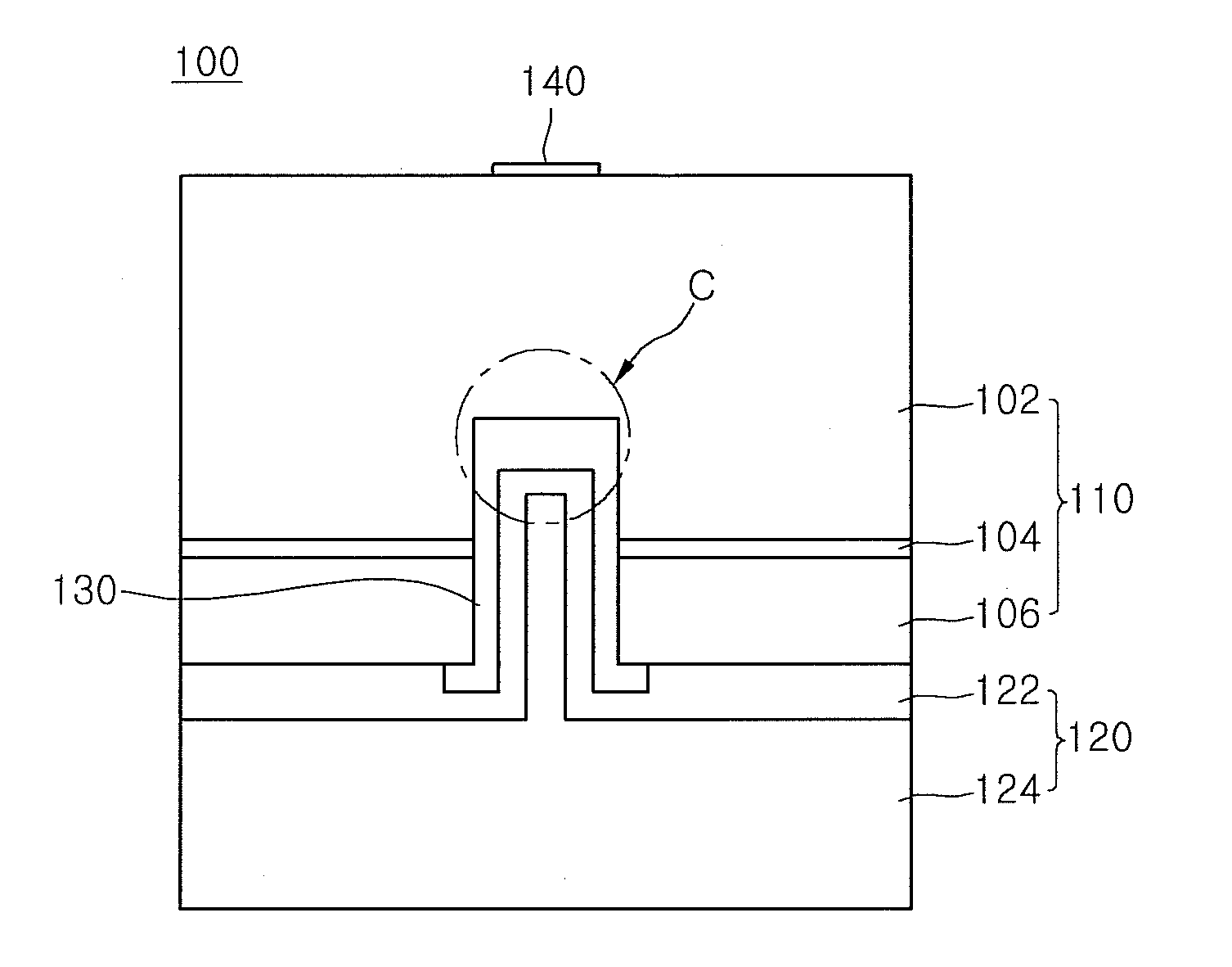
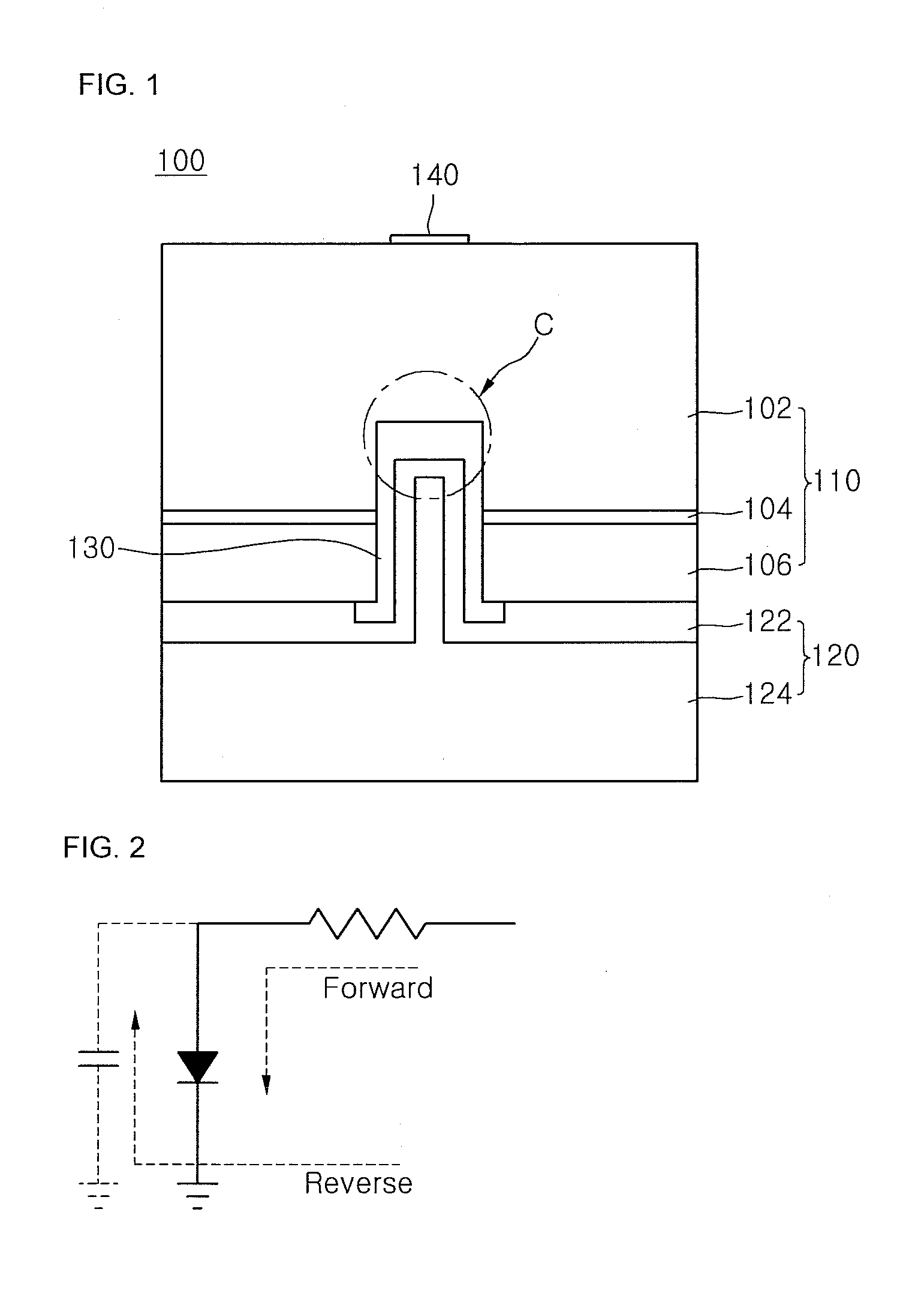
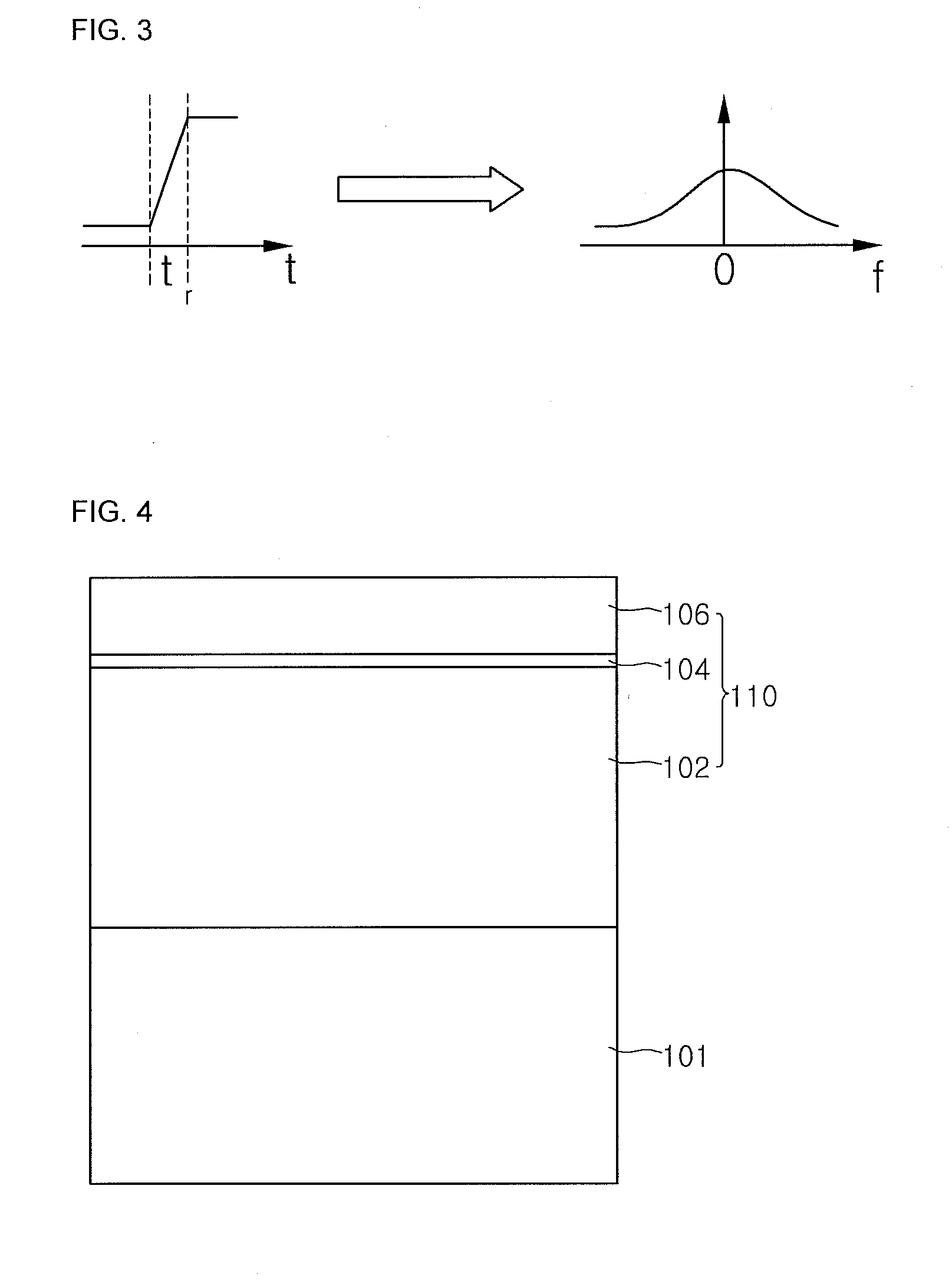
[0032]FIG. 1 is a sectional view showing a light emitting device according to a first embodiment, and FIG. 2 is a circuit diagram showing the light emitting device according to the embodiment.
[0033]The light emitting device according to the embodiment includes a light emitting structure 110 including a first conductive semiconductor layer 102, an active layer 104, and a second conductive semiconductor layer 106, a dielectric layer 130 formed in a cavity defined by removing a portion of the light emitting structure 110, and a second electrode layer 120 formed on the dielectric layer 130.
[0034]According to the embodiment, the first conductive semiconductor layer 102, the dielectric layer 130, and the second electrode layer 120 can carry out the function of a capacitor C. Although one capacitor C is shown in FIG. 1, the embodiment is not limited thereto. According to another embodiment, a plurality of capacitors may be provided.
[0035]In the light emitting device and a method of manufac...
PUM
 Abstract
Description
Claims
Application Information