Flat display panel, mother substrate for flat display panel, and method of manufacturing the flat display panel

a technology of flat display panel and mother substrate, which is applied in the manufacture of electrode systems, electric discharge tubes/lamps, instruments, etc., can solve the problems of deteriorating light emission efficiency and spoiled colors of emitted lights

Active Publication Date: 2012-04-26
SAMSUNG DISPLAY CO LTD
View PDF7 Cites 77 Cited by
  • Summary
  • Abstract
  • Description
  • Claims
  • Application Information

AI Technical Summary

Benefits of technology

[0010]The sealing member may be arranged in the non-display region and may surround the display region. The black matrix pattern in the non-display region may include a plurality of crossing black matrix patterns that cross the sealing region and that may be successively arranged in the sealing region. Black matrix patterns in the display region and black matrix regions in the non-display region may include different materials and compositions. Black matrix patterns in the display region and black matrix regions in the non-display region may be successively arranged and may include a same material. Black matrix patterns in the non-display region may protect a laser beam from being irradiated toward regions outside the sealing region when the laser beam is irradiated toward the sealing member. At least one black matrix pattern in the display region may have a lattice shape including a plurality of openings corresponding to sub-pixels. The second substrate may include color filters formed in the plurality of openings. The sealing member may be a frit. The first substrate may include a pixel circuit and an organic light emitting diode (OLED). The first substrate may include a pixel circuit, and a liquid crystal layer may be interposed between the first substrate and the second substrate.

Problems solved by technology

Furthermore, light emitting efficiency may be deteriorated and colors of emitted lights may be spoiled due to, e.g., spoils of liquid crystals and organic materials.

Method used


Image

  • Flat display panel, mother substrate for flat display panel, and method of manufacturing the flat display panel
  • Flat display panel, mother substrate for flat display panel, and method of manufacturing the flat display panel
  • Flat display panel, mother substrate for flat display panel, and method of manufacturing the flat display panel

Examples


Embodiment Construction

[0027]Korean Patent Application No. 10-2010-0103673, filed Oct. 22, 2010, in the Korean Intellectual Property Office, and entitled “Flat Display Panel, Mother Substrate For Flat Display Panel, and Method of Manufacturing the Flat Display Panel,” is incorporated by reference herein in its entirety.

[0028]Example embodiments will now be described more fully hereinafter with reference to the accompanying drawings; however, they may be embodied in different forms and should not be construed as limited to the embodiments set forth herein. Rather, these embodiments are provided so that this disclosure will be thorough and complete, and will fully convey the scope of the invention to those skilled in the art

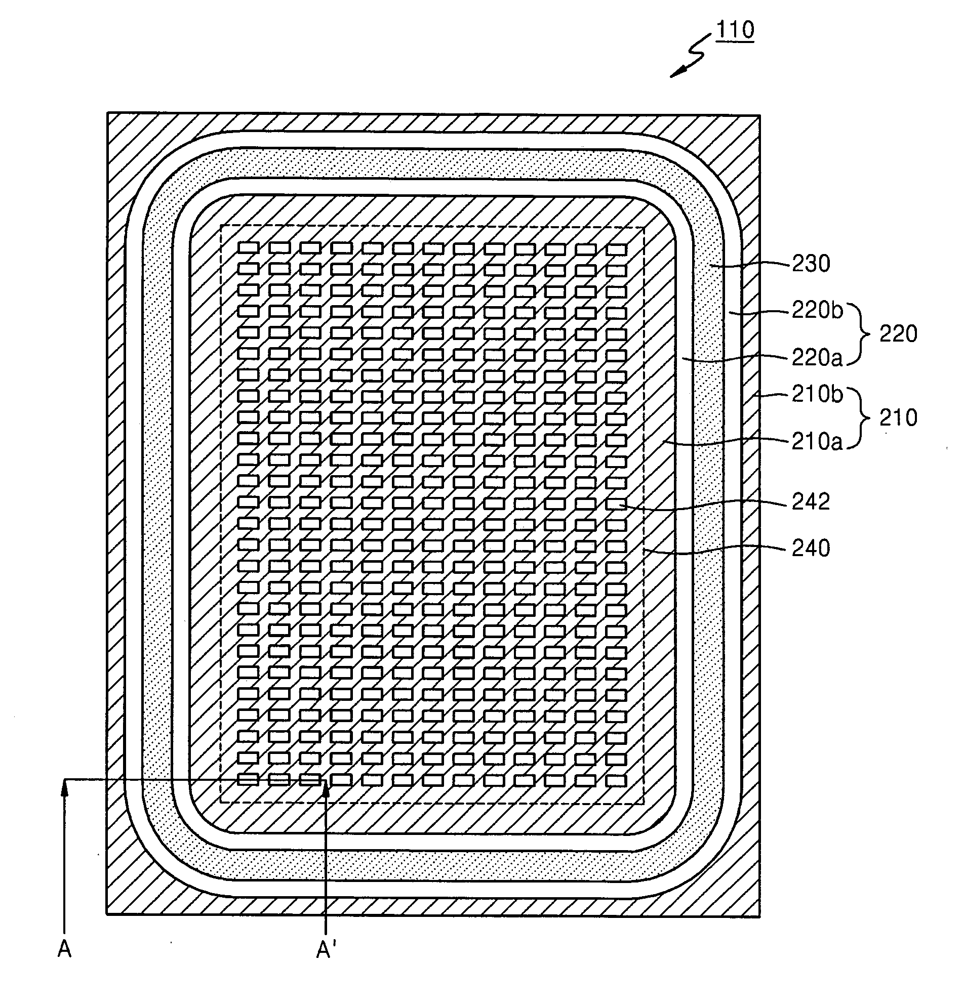
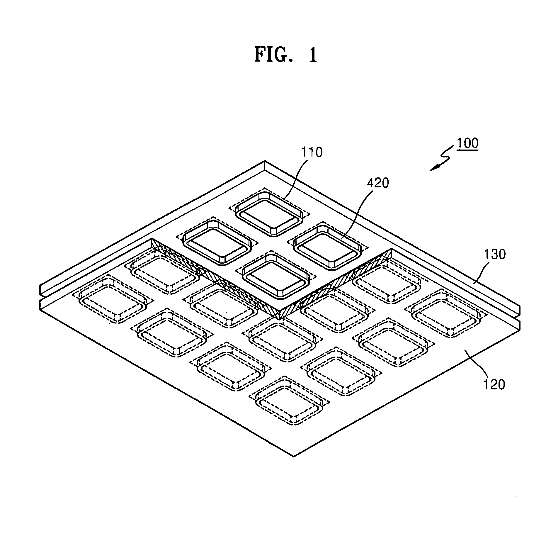
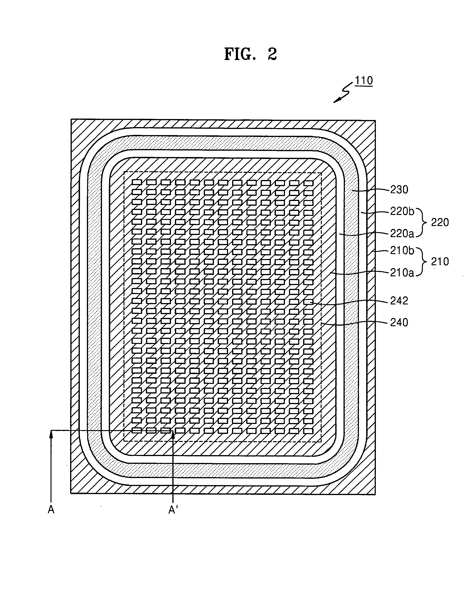
[0029]In the figures, the dimensions of layers and regions may be exaggerated for clarity of illustration. It will also be understood that when a layer or element is referred to as being “on” another layer or substrate, it can be directly on the other layer or substrate, or intervening l...


PUM

PropertyMeasurementUnit
widthsaaaaaaaaaa
compositionsaaaaaaaaaa
lattice shapeaaaaaaaaaa

Abstract

A flat display panel includes a first substrate and a second substrate, and the first and second substrates are sealed via a sealing member therebetween. The second substrate includes a display region and a non-display region. The display region and the non-display region include black matrix patterns, and the black matrix patterns have at least one opening in a sealing region of the second substrate. The sealing member is arranged in the sealing region

Description

BACKGROUND[0001]1. Field[0002]Embodiments relate to a flat display panel, a mother substrate for a flat display panel, and a method of manufacturing the flat display panel.[0003]2. Description of the Related Art[0004]Recently, conventional display devices tend to be replaced with portable and thin flat panel display device. Flat panel display devices may be embodied in various forms, such as liquid crystal display (LCD) devices, organic electroluminescent display devices, plasma display panels (PDP), or the like. A flat display panel included in a flat panel display device includes, e.g., a liquid crystal layer or organic light emitting diodes interposed between a first substrate and a second substrate. A pixel circuit may be formed on the first substrate.[0005]If moisture or oxygen in a surrounding environment permeates into such a flat display panel, lifespan of devices may be reduced due to, e.g., oxidization and a peeling-off of electrode materials. Furthermore, light emitting e...

Claims


Application Information

Patent Timeline
Patent Type & Authority Applications(United States)
IPC IPC(8): G02F1/1333H01J9/24G02B5/22
CPCG02B5/22H01J11/42H01J11/44G02F1/1339H01L51/5246H01L51/5284G02F1/133512H01J2211/444H10K50/8426H10K50/865H10K50/841
Inventor LEE, KYUNG-JUN
Owner SAMSUNG DISPLAY CO LTD
Why Eureka
Try Eureka