

Structural body and interconnect substrate
a technology of which is applied in the direction of cross-talk/noise/interference reduction, waveguide type devices, association of printed circuit non-printed electric components, etc., can solve the problems of increasing thickness of interconnect substrate, increasing manufacturing costs of ebg structural body and interconnect substrate, and reducing cost. , the effect of reducing thickness
- Summary
- Abstract
- Description
- Claims
- Application Information
AI Technical Summary
Benefits of technology
Problems solved by technology
Method used
Image

Examples
first embodiment
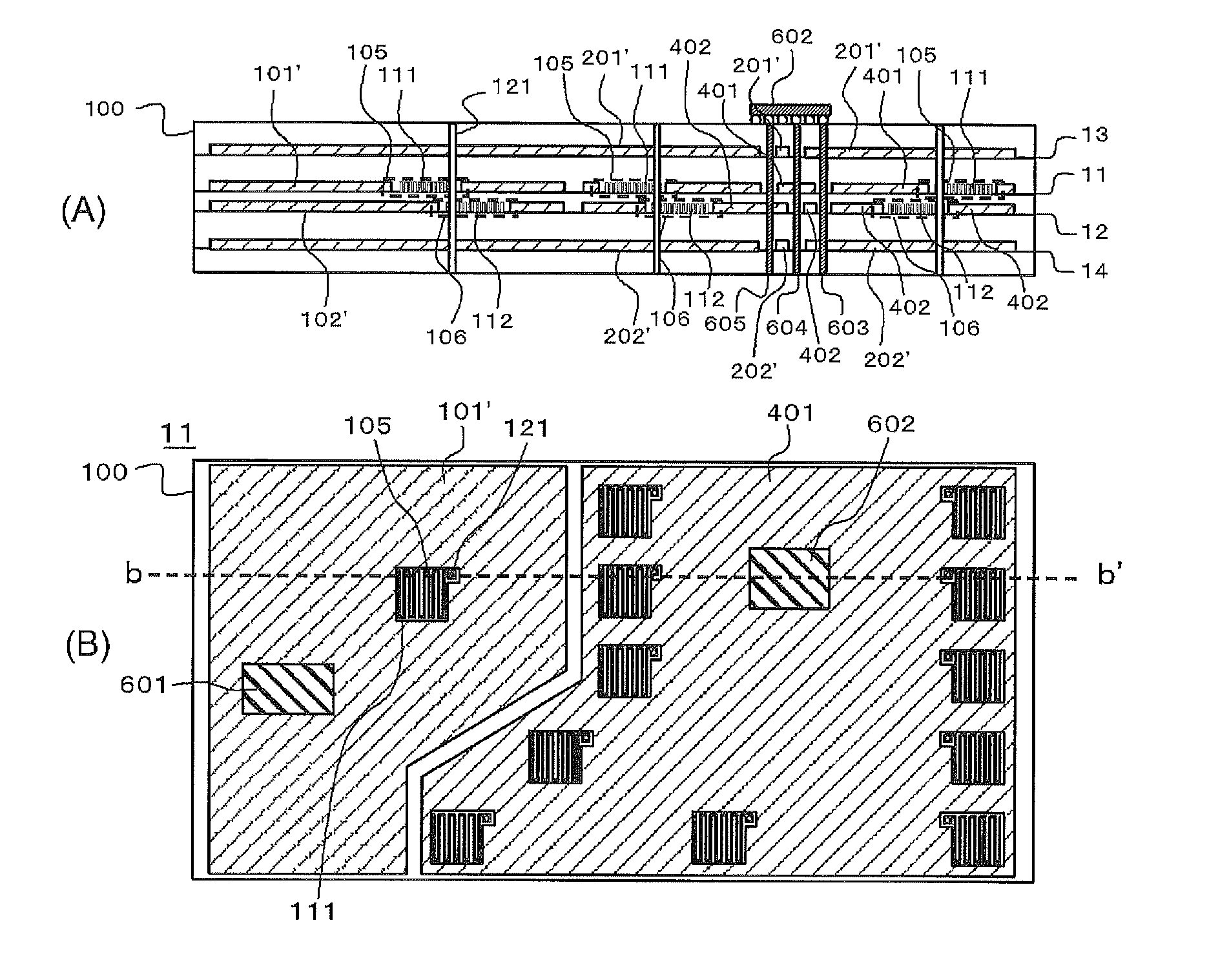
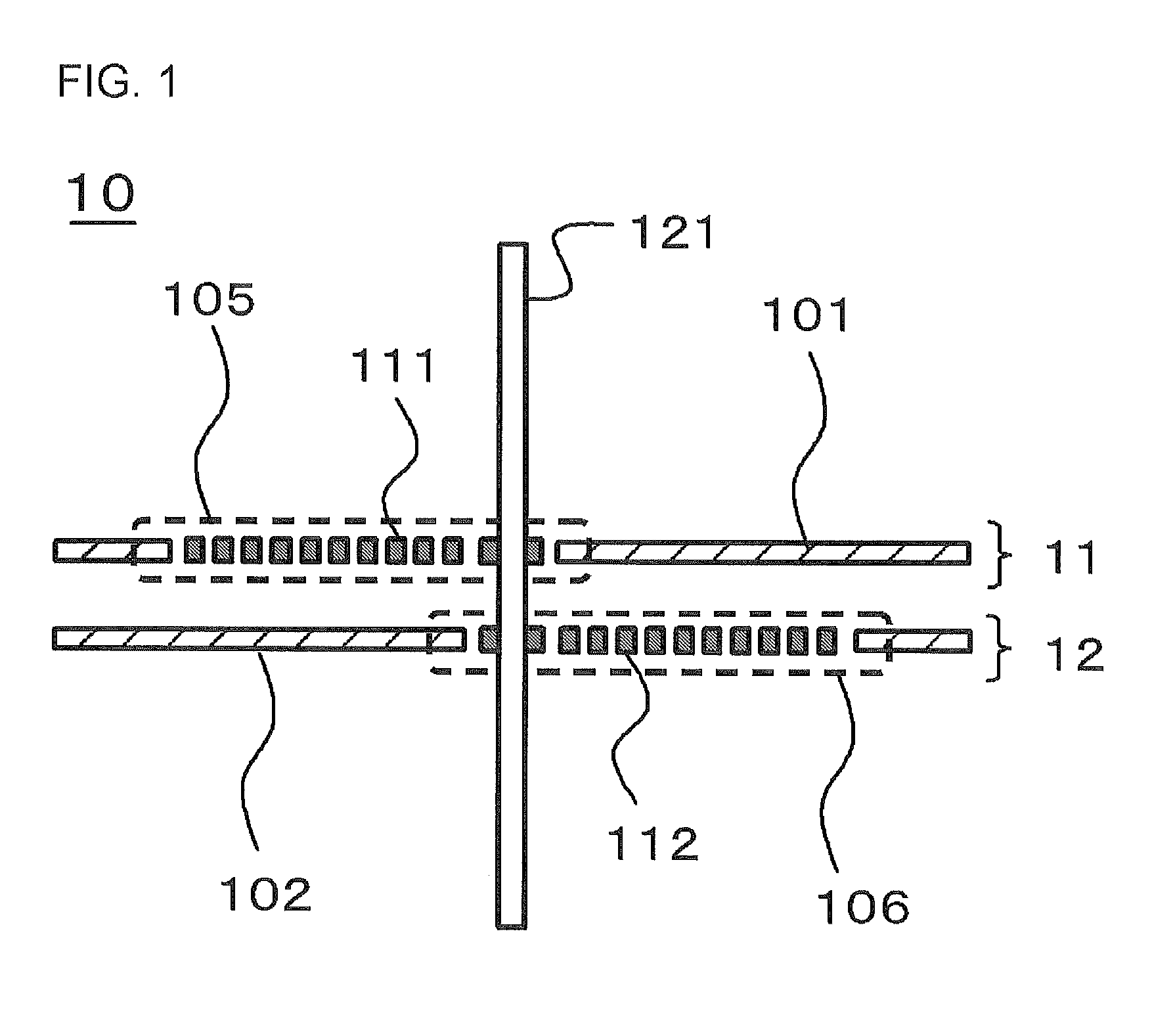
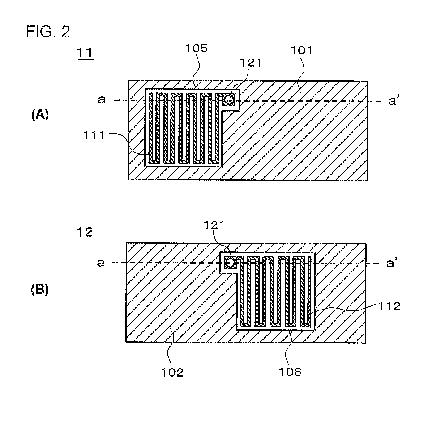
[0031]FIG. 1 is a cross-sectional view illustrating an example of a structural body 10 according to a first embodiment of the invention. FIG. 2 is a top view illustrating an example of the structural body 10 according to the first embodiment of the invention, FIG. 2(A) is a top view in an A layer 11, and FIG. 2(B) is a top view in a B layer 12. FIG. 1 is equivalent to a cross-sectional view taken along the line a-a′ in FIG. 2.
[0032]As shown in FIG. 1, the structural body 10 includes a first conductor 101, a second conductor 102, a first opening 105 and a second opening 106 which are provided in each of the first conductor 101 and the second conductor 102, a first interconnect 111 and a second interconnect 112 which are provided in each of the inside of the first opening 105 and the inside of the second opening 106, and a conductor via 121, passing through the first opening 105 and the second opening 106, which is insulated from the first conductor 101 and the second conductor 102.
[0...
second embodiment
[0054]FIG. 9 is a cross-sectional view illustrating an example of a configuration of the structural body 10 according to a second embodiment of the invention. The second embodiment has the same configuration as that of the structural body 10 according to the first embodiment, except that a third conductor 201 and a fourth conductor 202 are included.
[0055]Hereinafter, the structural body 10 will be described in detail. Meanwhile, a description of the same configuration as that of the first embodiment will be not repeated.
[0056]First, the third conductor 201 is disposed in a C layer 13 located above the A layer 11, and at least a portion thereof is opposite to the first conductor 101, for example, with a dielectric interposed therebetween. In addition, the third conductor 201 is connected to the conductor via 121.
[0057]Similarly, the fourth conductor 202 is disposed in a D layer 14 located below the B layer 12, and at least a portion thereof is opposite to the second conductor 102, fo...
third embodiment
[0063]FIG. 10 is a cross-sectional view illustrating an example of a configuration of the structural body 10 according to a third embodiment of the invention. FIG. 11 is a top view illustrating an example of the structural body 10 according to the third embodiment of the invention. FIG. 11(A) is a top view in the C layer 13, and FIG. 11(B) is a top view in the D layer 14. FIG. 10 is equivalent to a cross-sectional view taken along the line a-a′ in FIG. 11.
[0064]The third embodiment has the same configuration as that of the structural body 10 according to the second embodiment, except that the third conductor 201 and the fourth conductor 202 have an opening.
[0065]As shown in FIGS. 10 and 11(A), the third conductor 201 includes a third opening 301 in a region overlapping the first interconnect 111 when seen in a plan view. In FIG. 11(A), in order to show the positional relationship between the first interconnect 111 and the third opening 301, the first interconnect 111 which is not pr...
PUM
 Abstract
Description
Claims
Application Information