Array substrate and relevant display panel

a substrate and substrate technology, applied in the field of liquid crystal substrates and relevant display panels, can solve the problems of high manufacturing cost, high manufacturing cost, fragile and lacking flexibility of indium in the ito, etc., and achieve the effect of low manufacturing cost and high manufacturing cos

Inactive Publication Date: 2013-09-19
SHENZHEN CHINA STAR OPTOELECTRONICS TECH CO LTD
View PDF5 Cites 2 Cited by
  • Summary
  • Abstract
  • Description
  • Claims
  • Application Information

AI Technical Summary

Benefits of technology

[0007]An objective of the present invention embodiments is to provide a array substrate having low manufacture cost to ...

Problems solved by technology

However, Indium in the ITO is expensive, fragile ...

Method used


Image

  • Array substrate and relevant display panel
  • Array substrate and relevant display panel

Examples


Embodiment Construction

[0030]The following descriptions for the respective embodiments are specific embodiments capable of being implemented for illustrations of the present invention with referring to appended figures. For example, the terms of up, down, front, rear, left, right, interior, exterior, side, etcetera are merely directions of referring to appended figures. Therefore, the wordings of directions are employed for explaining and understanding the present invention but not limitations thereto.

[0031]In figures, the elements with similar structures are indicated by the same number.

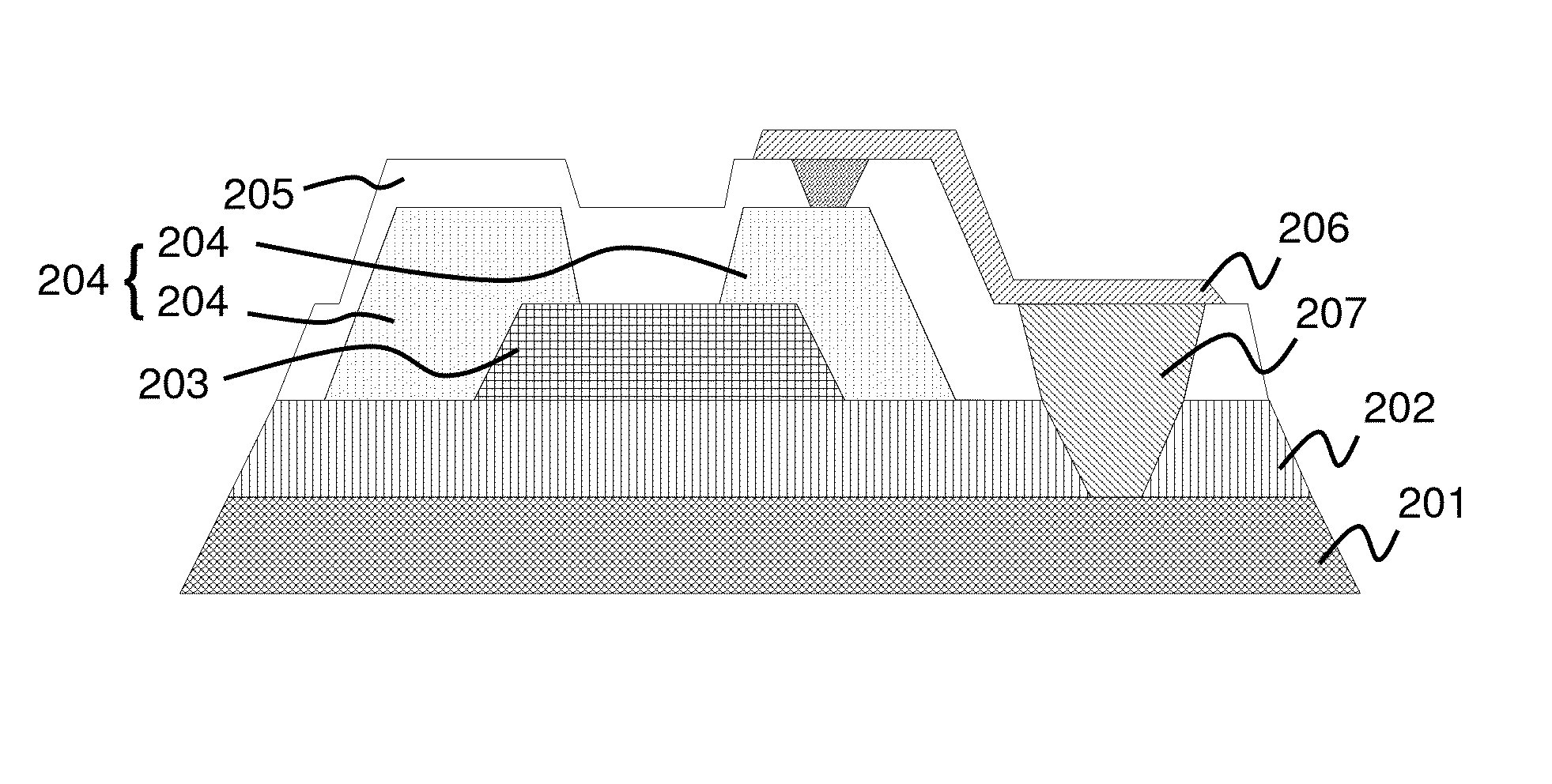
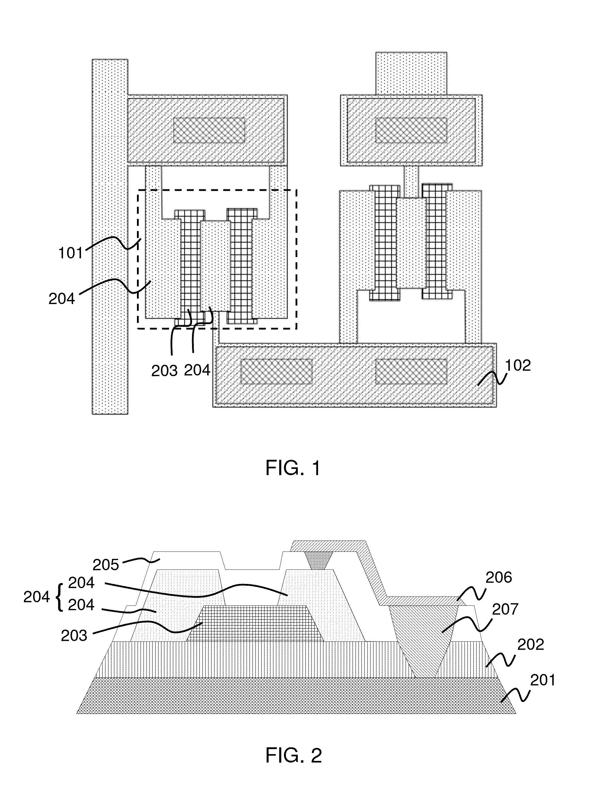
[0032]As shown in FIG. 1 and FIG. 2, FIG. 1 depicts a planar construction diagram of a preferable embodiment according to the array substrate of the present invention. FIG. 2 depicts a construction diagram of respective functioned layers in a preferable embodiment according to the array substrate of the present invention. The array substrate shown in FIG. 1 has a display area and a peripheral circuit area outside the disp...


PUM


Abstract

Disclosed are an array substrate and a relevant display panel. The array substrate has a display area and a peripheral circuit area outside the display area. The array substrate comprises a pixel array and a peripheral circuit. The pixel array comprises thin film transistors and pixel electrodes. The pixel electrodes are graphene thin films. The array substrate and the relevant display panel according to the present invention have low manufacture cost.

Description

BACKGROUND OF THE INVENTION[0001]1. Field of the Invention[0002]The present invention generally relates to a liquid crystal display field, and more particularly to a liquid crystal substrate and a relevant display panel.[0003]2. Description of Prior Art[0004]With development of technology, kinds of electronic products have become an important portion of human beings' lives. LCD (Liquid crystal display) panel is the main component of the multimedia electronic product. The present TFT-LCD panel provides advantages of power saving, no radiation, small size, lower power consumption, less occupation space, flat square, high resolution, stable image quality and etc. Accordingly, it has been replaced the traditional CRT display (cathode ray tube display) and therefore is widely applied in display panels of the electronic products, such as cell phones, screens, digital televisions, laptop computers and etc.[0005]Along with the rapid development of skills related with liquid display panels. ...

Claims


Application Information

Patent Timeline
IPC IPC(8): H01L27/15
CPCG02F1/13439H01L27/124
Inventor WANG, YEWEN
Owner SHENZHEN CHINA STAR OPTOELECTRONICS TECH CO LTD
Why Eureka
Try Eureka