Semiconductor system and operating method thereof

a technology of semiconductors and operating methods, applied in the direction of unauthorized memory use protection, memory adressing/allocation/relocation, instruments, etc., can solve the problems of sudden power failure, unexpected power supply stoppage, etc., and achieve the effect of increasing the area of the device and reducing the tim

Active Publication Date: 2015-04-30
SK HYNIX INC
View PDF2 Cites 0 Cited by
  • Summary
  • Abstract
  • Description
  • Claims
  • Application Information

AI Technical Summary

Benefits of technology

[0008]The present invention has been made in an effort to provide a semiconductor system capable of, when a sudden power fail is caused, restoring data, which is programmed in a semiconductor memory device before the sudden power fail, in a reduced time without increasing the area of a device for restoring the data, and an operating method thereof.

Problems solved by technology

In the meantime, a sudden power fail may be caused during the operation of the semiconductor system.
The sudden power fail means a phenomenon in which the supply of power is unexpectedly stopped.

Method used


Image

  • Semiconductor system and operating method thereof
  • Semiconductor system and operating method thereof
  • Semiconductor system and operating method thereof

Examples


Embodiment Construction

[0024]Hereinafter, an embodiment of the present invention will be described with reference to the accompanying drawings in detail. However, the present invention is not limited to an embodiment disclosed below and may be implemented in various forms and the scope of the present invention is not limited to the following embodiments. Rather, the embodiment is provided to more sincerely and fully disclose the present invention and to completely transfer the spirit of the present invention to those skilled in the art to which the present invention pertains, and the scope of the present invention should be understood by the claims of the present invention.

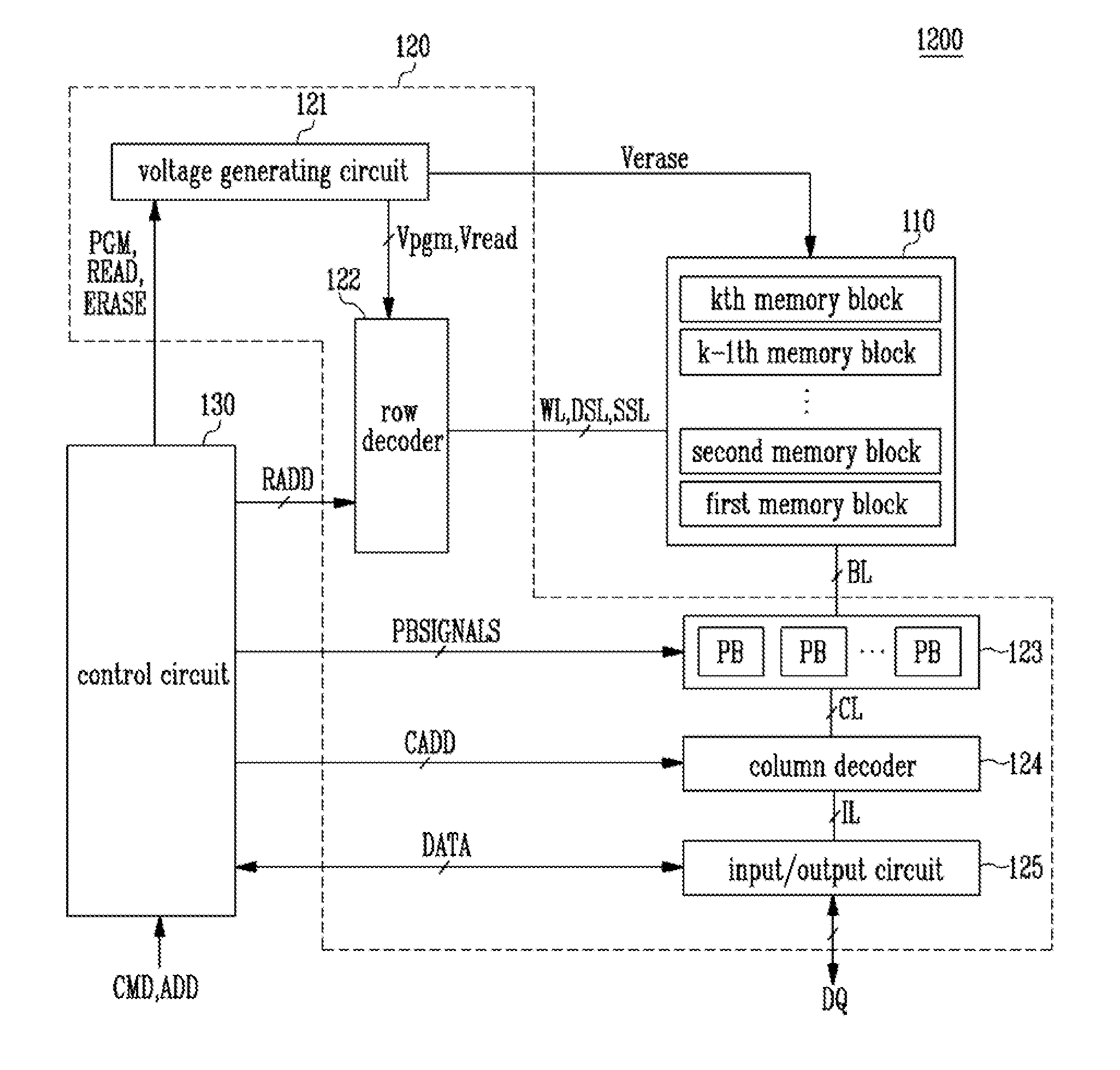
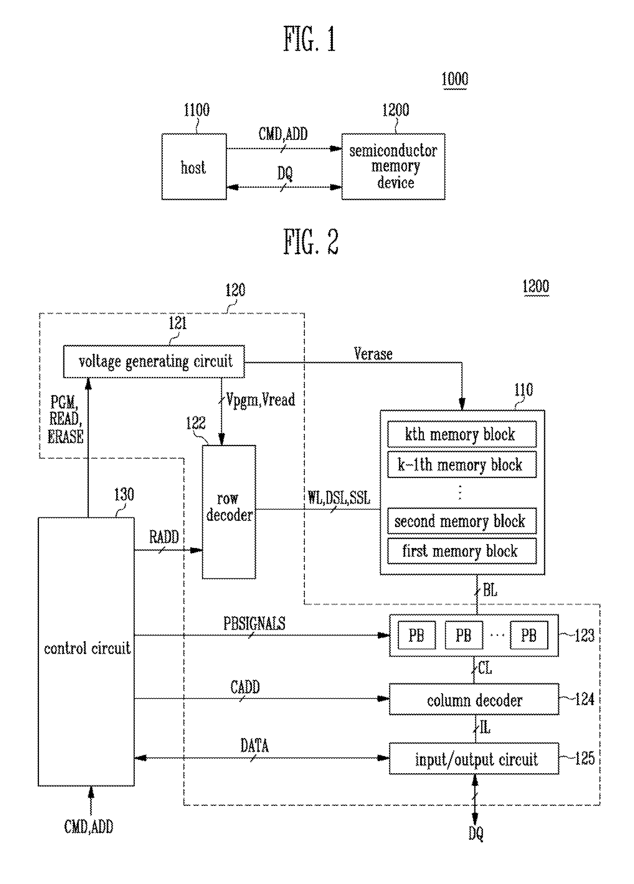
[0025]FIG. 1 is a block diagram illustrating a semiconductor system according to an embodiment of the present invention.

[0026]Referring to FIG. 1, the semiconductor system 1000 includes a host 1100 and a semiconductor memory device 1200. The host 1100 outputs operation command signals CMD, addresses ADD, and data DQ for controlling the ...


PUM


Abstract

A semiconductor system includes a semiconductor memory device suitable for storing data, and a host suitable for controlling the semiconductor memory device in response to an external command signal, in which the semiconductor memory device includes a buffer block suitable for storing first data programmed under control of the host, and a main block suitable for storing the second data programmed under control of the host or a copy of the first data stored in the buffer block at a sudden power fail.

Description

CROSS-REFERENCE TO RELATED APPLICATION[0001]The present application claims priority of Korean patent application number 10-2013-0128491, filed on Oct. 28, 2013, in the Korean Intellectual Property Office, the entire disclosure of which is incorporated herein by reference in its entirety.BACKGROUND[0002]1. Field of Invention[0003]Various embodiments of the present invention relate to a semiconductor system and an operating method thereof, and more particularly, to a semiconductor system for restoring data when a sudden power fail is caused and an operating method thereof.[0004]2. Description of Related Art[0005]A semiconductor system includes a semiconductor memory device configured to store data, and a host configured to control the semiconductor memory device. The host transfers command signals, and addresses for program, read, and erase operations to the semiconductor memory device, and the semiconductor memory device performs the program, read, and erase operations in response to...

Claims


Application Information

Patent Timeline
Patent Type & Authority Applications(United States)
IPC IPC(8): G06F3/06G06F12/02
CPCG06F3/0619G06F3/065G06F2212/702G06F12/0253G06F3/0679G06F11/1441G06F11/14G06F12/14G06F12/16
Inventor KIM, EUI JIN
Owner SK HYNIX INC
Why Eureka
Try Eureka